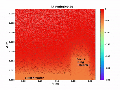
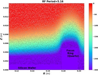
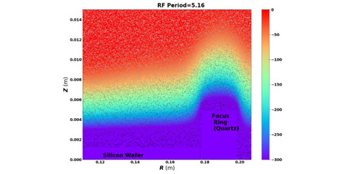
A common use of low-temperature plasmas is in the area known as wafer etching, in which plasma impacts a wafer to etch various microelectronic devices such as memory. One advantage to this method is that the etching is much cleaner and uniform, resulting in better quality control. The ions are the plasma species that do the etching due to their larger mass. We broadly call this application “plasma processing.” In plasma processing, the plasma is generated using capacitively coupled (CCP) or inductively coupled methods (ICP), or a combination of both. In our example, we assume a pre-loaded plasma in the simulation.
Kinetically Model Plasma Species
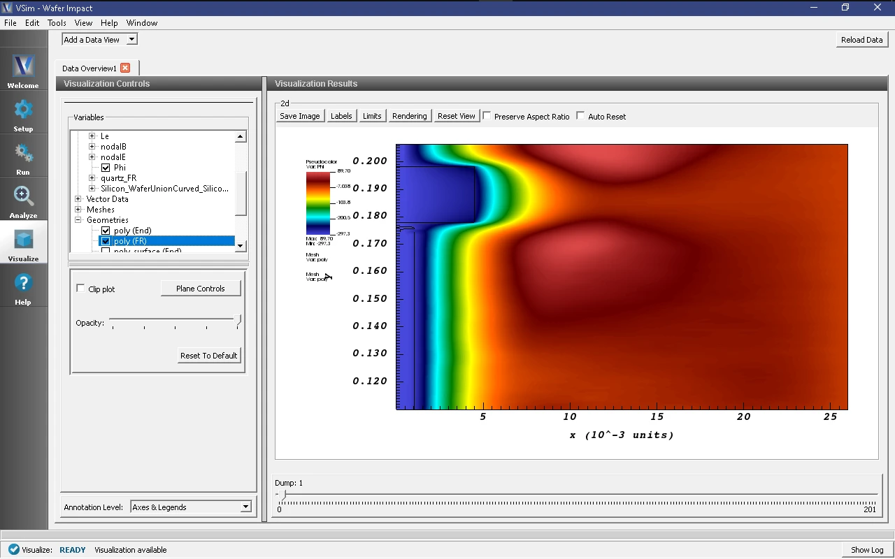
Using VSim, you can kinetically model all plasma species to correctly calculate the electric field at each time step. This is essential to correctly compute the sheath electric field, which directly affects the ion’s impact energy and angle. You can use VSim’s intuitive interface to create and visualize the wafer and surrounding dielectrics, which help create a more uniform wafer.
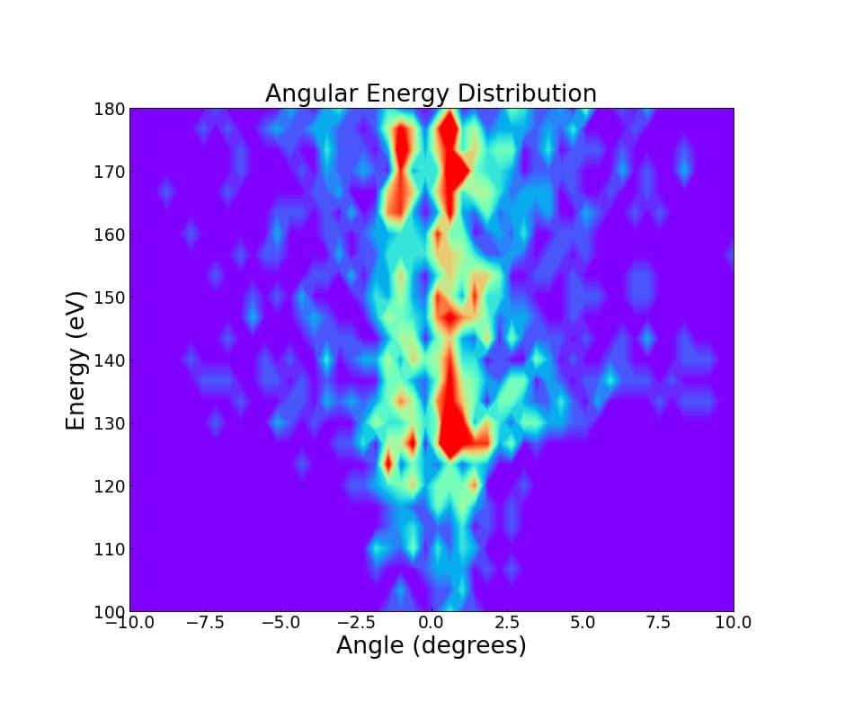
Simulate angle-energy distribution
Once the simulation is finished, you can compute the angle-energy distribution functions using our custom analyzer called computeAED.py. This analyzer bins the data from any kinetic species (ions or electrons) in energy and angle along any surface, such as the wafer. You can also bin in time according to your chosen time interval.
This website or its third-party tools process personal data.In case of sale of your personal information, you may opt out by using the link Do not sell my personal information.
This website uses cookies to improve your experience while you navigate through the website. Out of these, the cookies that are categorized as necessary are stored on your browser as they are essential for the working of basic functionalities of the website. We also use third-party cookies that help us analyze and understand how you use this website. These cookies will be stored in your browser only with your consent. You also have the option to opt-out of these cookies. But opting out of some of these cookies may affect your browsing experience.
Necessary cookies are absolutely essential for the website to function properly. These cookies ensure basic functionalities and security features of the website, anonymously.
Cookie
Duration
Description
cookielawinfo-checkbox-analytics
11 months
This cookie is set by GDPR Cookie Consent plugin. The cookie is used to store the user consent for the cookies in the category "Analytics".
cookielawinfo-checkbox-functional
11 months
The cookie is set by GDPR cookie consent to record the user consent for the cookies in the category "Functional".
cookielawinfo-checkbox-necessary
11 months
This cookie is set by GDPR Cookie Consent plugin. The cookies is used to store the user consent for the cookies in the category "Necessary".
cookielawinfo-checkbox-others
11 months
This cookie is set by GDPR Cookie Consent plugin. The cookie is used to store the user consent for the cookies in the category "Other.
cookielawinfo-checkbox-performance
11 months
This cookie is set by GDPR Cookie Consent plugin. The cookie is used to store the user consent for the cookies in the category "Performance".
viewed_cookie_policy
11 months
The cookie is set by the GDPR Cookie Consent plugin and is used to store whether or not user has consented to the use of cookies. It does not store any personal data.
Functional cookies help to perform certain functionalities like sharing the content of the website on social media platforms, collect feedbacks, and other third-party features.
Performance cookies are used to understand and analyze the key performance indexes of the website which helps in delivering a better user experience for the visitors.
Analytical cookies are used to understand how visitors interact with the website. These cookies help provide information on metrics the number of visitors, bounce rate, traffic source, etc.
Advertisement cookies are used to provide visitors with relevant ads and marketing campaigns. These cookies track visitors across websites and collect information to provide customized ads.