Field Emitter Array (fieldEmitterArray.sdf)
Keywords:
- field-induced emission, particle beam, FEA, emitter array, Fouler-Nordheim, space charge
Problem Description
Obtaining high currents and high current densities via electron emission from cold cathodes is a high demand for scientists and engineers. Field emitter arrays (FEAs) operate via field-induced particle emission from very thin cathodes and are highly efficient. For this reason, they have been widely studied via experimental methods.
This VSim for Vacuum Electronics example illustrates how to setup a 3x3 FEA. VSim uses a cut-cell field emitter following a space-charge corrected Fowler-Nordheim emission model [1]. VSim has the capability of managing geometry structures at the micron and even nanometer range, effectively meshing single emitters and emitter arrays. In addition, VSim also models dielectric to second-order accuracy, making it possible to include dielectrics in the FEA design.
This simulation can be run with a VSimVE license.
Opening the Simulation
The Field Emitter Array example is accessed from within VSimComposer by the following actions:
Select the New → From Example… menu item in the File menu.
In the resulting Examples window expand the VSim for Vacuum Electronics option.
Expand the Radiation Generation option.
Select Field Emitter Array and press the Choose button.
In the resulting dialog, create a New Folder if desired, then press the Save button to create a copy of this example.
The resulting Setup Window is shown Fig. 409.
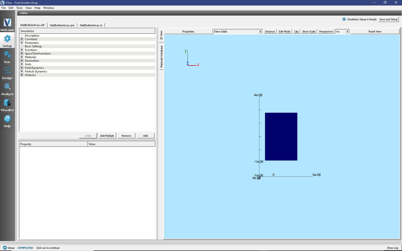
Fig. 409 Setup Window for the Field Emitter Array example.
Simulation Properties
The simulated device is a 3x3 field emission array with a dielectric substrate. In order to simplify the setup of the geometry, each emitter tip was set up as a thin cylinder of length of 0.55 microns and a radius of 0.05 microns. The emitter tips are 0.05 microns deep in inside the gate openings which are 0.15 microns in radius. The metal gate thickness is 0.1 microns. The distance between the emitter and the cavity wall is 1.15 microns. The distance between the centers of adjacent emitters is 1.00 microns. The metal gate was topped with a dielectric layer with a thickness of 0.1 microns. Alumina was set for the dielectric material. The voltage between the cathode and the gate was set to 100 V, while the gate to anode voltage was set to 4000 V. These voltages were set through a feedback algorithm.
Running the Simulation
Once finished with the setup, continue as follows:
Proceed to the Run Window by pressing the Run button in the navigation column out left.
To run the file, click on the Run button in the upper left corner of the Logs and Output Files pane. You will see the output of the run in that pane. The run has completed successfully when you see the output, “Engine completed successfully.” This is shown in Fig. 410.
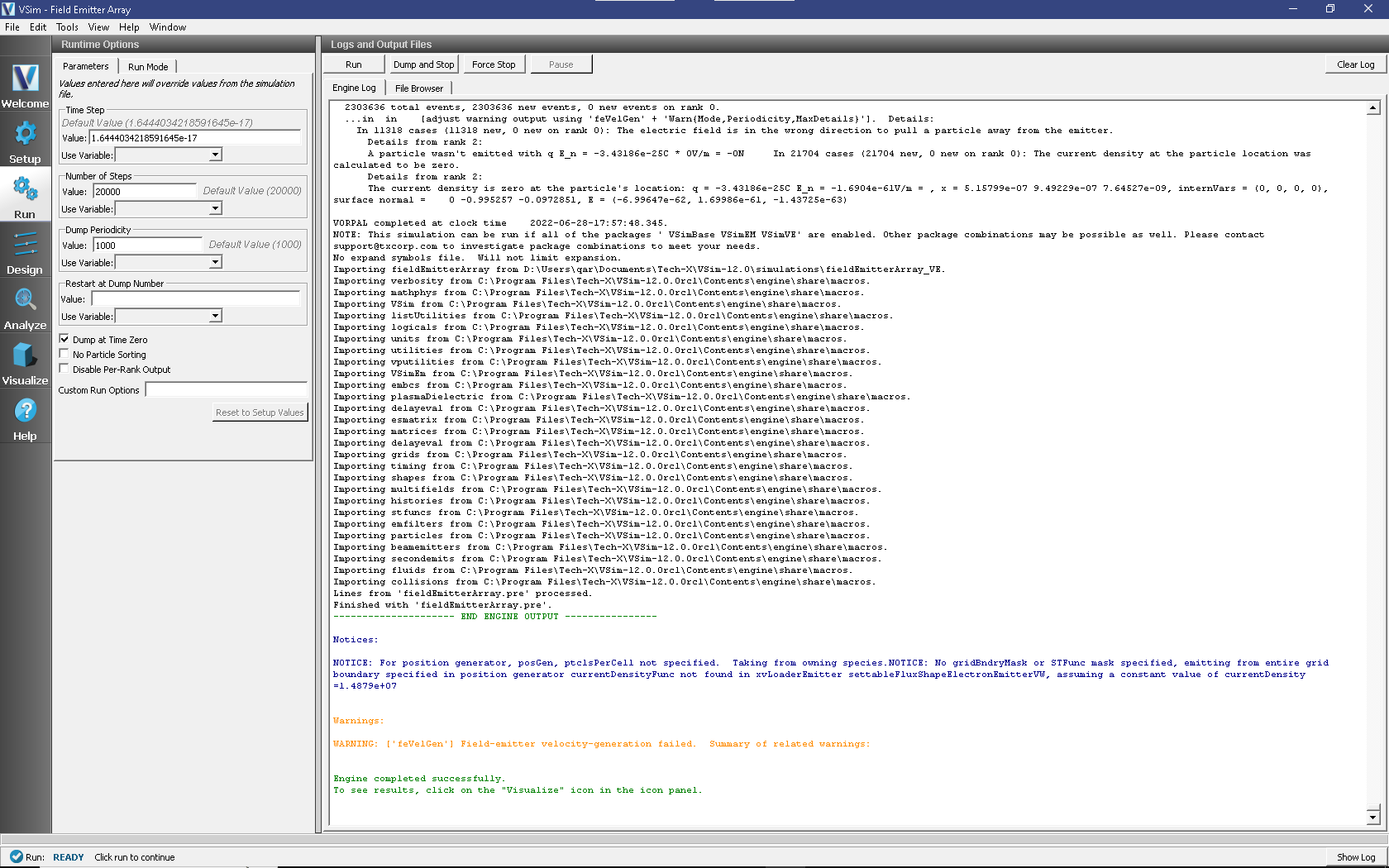
Fig. 410 The Run Window at the end of execution.
Visualizing the Results
After performing the above actions, the results can be visualized as follows:
Proceed to the Visualize Window by pressing the Visualize button in the navigation column.
From the Data View dropdown menu, select Data Overview.
In the variables tree, expand Particle Data.
Select electrons.
In the variables tree, expand Geometries.
Select poly_surface (fieldEmitterArrayPecShapes).
Check the Clip plot box and select the Plane Controls button.
Under Clip Plane Normal select X (plane normal to x-axis).
Under Origin of Normal Vector type 1.7e-6 and click Ok.
Select poly_surface (substrateGeomSolid).
Check the Clip plot box and select the Plane Controls button.
Under Clip Plane Normal select X (plane normal to x-axis).
Under Origin of Normal Vector type 1.7e-6 and click Ok.
In the bottom of the right pane, move the dump slide forward in time.
The resulting visualization is shown in Fig. 411.
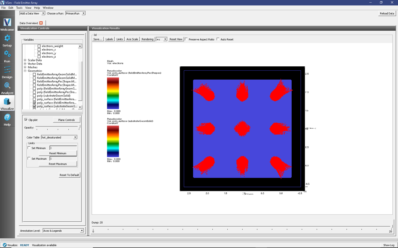
Fig. 411 Electron beams originating from the emitter tips behind the dielectric substrate.
To perform an analysis of the axial electric field, proceed as follows:
Proceed to the Visualize Window by pressing the Visualize button in the navigation column.
From the Data View dropdown menu, select Field Analysis.
Under Field select E_x from the drop-down menu.
Select Log Scale Color Table.
Under Intercept input 6.5e-7.
Under Layout select Side-by-side 2d/1d.
Click Perform Lineout
Select Controls on the 2D plot and select Colors. Click Fix Maximum with the value 1e+10.
In the bottom of the right pane, move the dump slide forward in time.
The resulting visualization is shown in Fig. 412.
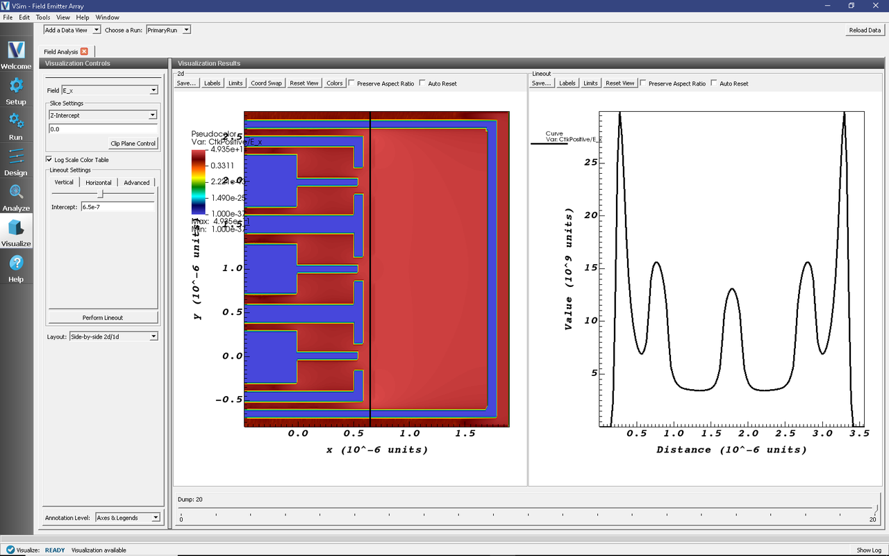
Fig. 412 2D and 1D studies of the electric field which is highly space-charge dominated. The 1D lineout was performed along the dielectric substrate.
To visualize the electron energy and current histories, proceed as follows:
Proceed to the Visualize Window by pressing the Visualize button in the navigation column.
From the Data View dropdown menu, select History.
The resulting visualization is shown in Fig. 413.
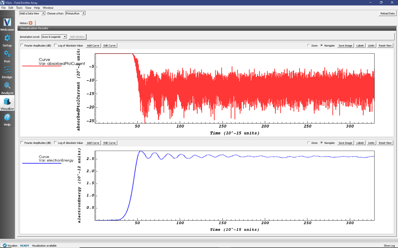
Fig. 413 The histories of the emitted and absorbed particle current, and the electron beam energies.
To visualize the electron Px-x phase space, proceed as follows:
Proceed to the Visualize Window by pressing the Visualize button in the navigation column.
From the Data View dropdown menu, select Phase Space.
For the X-axis, select electrons_x.
For the Y-axis, select electrons_ux.
Click Draw.
Move the dump slider further in time.
The resulting visualization is shown in Fig. 414.
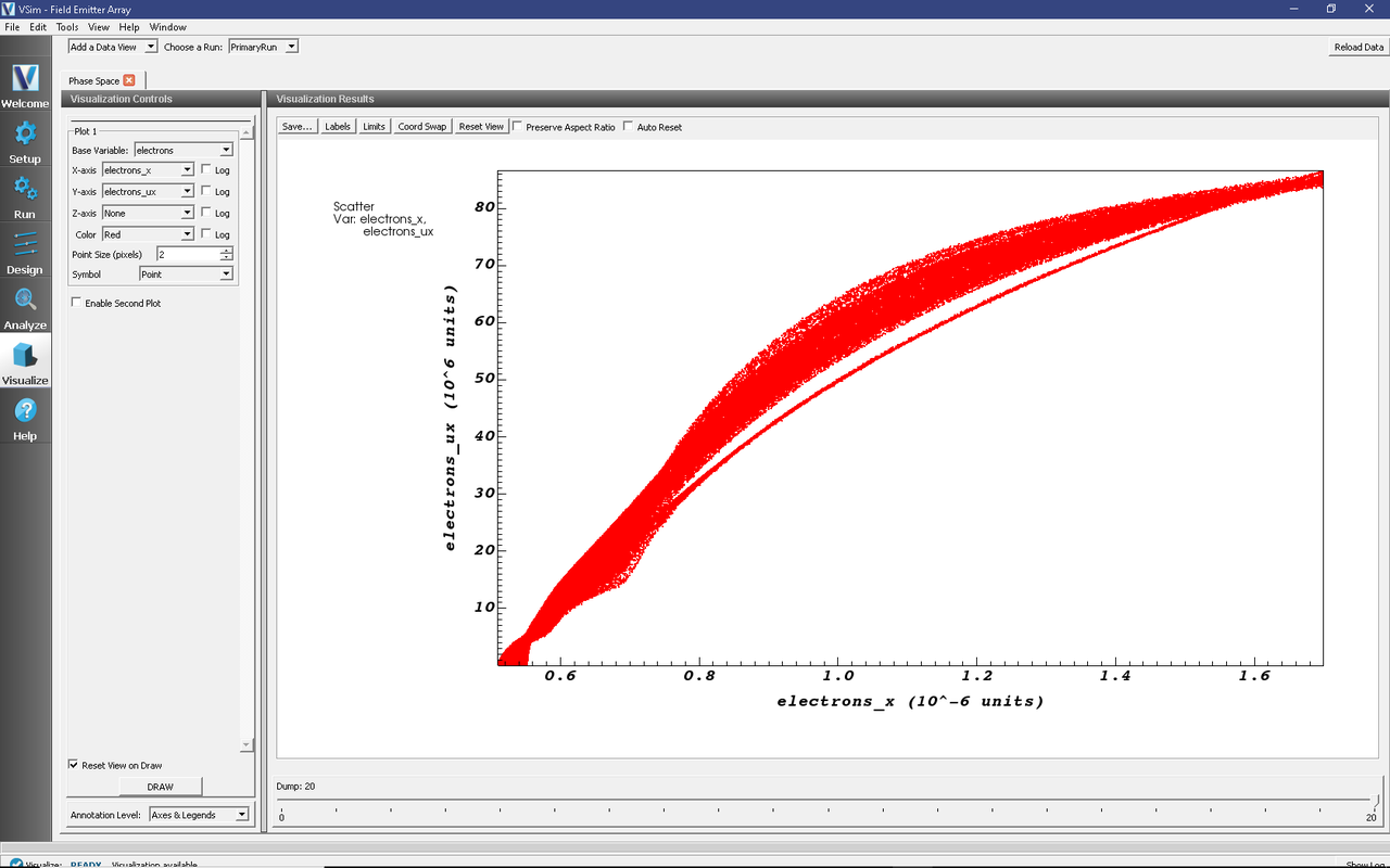
Fig. 414 The distribution of field-emitted electrons on the Px-x phase space.
Fig. 411 shows the first results: narrow strong beams of particles emitted from the tips of the 9 emitters. In addition, Fig. 412 shows the axial component of the electric field which is highly space-charge dominated. A lineout measurement is performed at the location of the dielectric substrate (right-hand image). The histories of the emitted and absorbed particle currents and the electron energy are shown in Fig. 413. Lastly, the distribution of field-emitted electron on the Px-x phase space is shown in Fig. 414.
Further Experiments
One of the first tests that can be performed easily using this simulation is to investigave how the electron emission behaves when changing the anode and cathode voltages. These voltages are defined in the setup element tree under ANODE_VOLTAGE and DC_BIAS, respectively.
Another study can be performed by changing the properties of the dielectric substrate and investigating the resulting effects. The user can edit the dielectric material properties directly in the setup window under “Materials” by selecting the material and then manually changing the property values (conductivity, permittivity, etc.) in the pane below.