Inter Layer Slope Coupler (interLayerSlopeCoupler.sdf)
Keywords:
- S Parameter, Mode Launcher, MAL, Guided Mode, Photonic Device, Semiconductor
Problem Description
The Inter Layer Slope Coupler uses a sloped waveguide to connect two different layers of a photonic chip. The purpose of creating multiple layers on 3D space in a single wafer is to increase the density of a compute system. The challenge with designing a multi-layer chip is minimizing the amount of loss due to scattering when moving the signal between layers. This device uses 3 silicon waveguides that are surrounded by a silicon dioxide layer.
This example makes use of a “Photonics simulation template” intended to allow for rapid setup of any passive photonic device, provided the ports are aligned with the X-Axis. Matched Absorbing Layers (MALs) are used to dampen the E, B and D fields near the boundary of the simulation.
The fundamental guided mode profile is calculated and launched as a wide band pulse down the input waveguide. Upon completion of the simulation, a post-processing analyzer is used to calculate the S-parameters for all of the wavelengths in the pulse.
This simulation can be performed with a XSimEM license.
Opening the Simulation
The Inter Layer Slope Coupler example is accessed from within XSimComposer by the following actions:
Select the New → From Example… menu item in the File menu.
In the resulting Examples window expand the XSim for Electromagnetics option.
Expand the Photonics option.
Select Inter Layer Slope Coupler and press the Choose button.
In the resulting dialog, create a New Folder if desired, and press the Save button to create a copy of this example.
All of the properties and values that create the simulation are available in the Setup Window as shown in Fig. 298. You can expand the tree elements and navigate through the various properties. The right pane shows a 3D view of the geometry, as well as the grid, if actively shown. To show or hide the grid, expand the Grid element and select or deselect the box next to Grid.
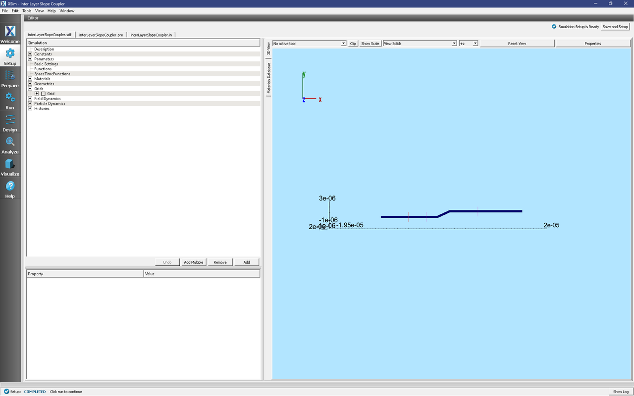
Fig. 298 The Setup window for the Inter Layer Slope Coupler example showing the 3D geometry.
Simulation Properties
This example contains a number of Constants defined to make the simulation easily modifiable.
General Simulation Constants:
WGWIDTH = The width of all 3 of the waveguides used to make the geometry.
HEIGHT = The height of all 3 of the waveguides.
LENGTHINOUT = The length of the input and output waveguides.
RISEANGDEG = The slope angle in degrees.
CELLSPERWAVELENGTH = The number of cells to use to simulate the center wavelength.
WAVELENGTH = The center wavelength of the pulse.
WAVELENGTH_HI = The maximum wavelength of the pulse.
WAVELENGTH_LOW = The minimum wavelength of the pulse.
This simulation applies a wide frequency band signal to the fundamental spatial mode profile. The spatial profile is calculated and imported in to the waveguide mode launcher (waveguideModeLauncher0 under Field Dynamics → CurrentDistributions). The temporal profile is also defined in the waveguide mode launcher under the Temporal Profile option.
The Materials section contains just Silicon. This allows it to be assigned to the pieces of the 3D geometry. The surrounding silicon dioxide is simulated by setting the background permittivity option under Basic Settings to 3.9.
In Field Dynamics there are FieldBoundaryConditions which set the boundary conditions of the simulation. In photonics simulations, Matched Absorbing Layers (MALs), are the most stable boundary conditions for preventing reflections.
Under Basic Settings you can see that the dielectric solver is set to permittivity averaging. This feature enables second order accuracy for simulations using dielectrics.
Running the Simulation
When you have saved the setup, continue as follows:
Proceed to the run window by pressing the Run button in the left column of buttons.
Check that you are using these run parameters:
Time Step: 5.680122342760484e-17
Number of Steps: 12000
Dump Periodicity: 1200
Dump at Time Zero: Checked
Click on the Run button in the upper left corner of the right pane.
You will see the output of the run in the right pane. The run has completed when you see the output, “Engine completed successfully”. As seen in Fig. 299.
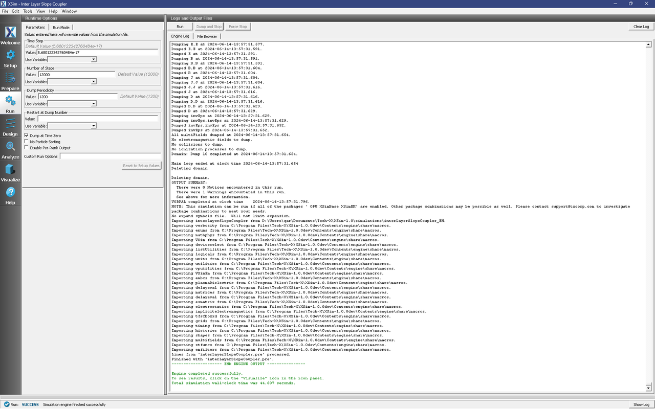
Fig. 299 Run window at completion.
Analyzing the Results
Using post analysis scripts, one can extract the S-parameters. This simulation uses 2 “EM Field on Plane” histories (inputPort, outputPort) and this data is used to calculate S-parameters between these 2 locations using the analysis script computeSParamsFromHists.py.
Follow these steps:
Proceed to the Analyze Window by clicking the Analyze button on the left.
Select computeSParamsFromHists.py and click Open under the list.
Now update the analyzer fields accordingly.
simulationName = interLayerSlopeCoupler
firstStep = 0
lastStep = 12000
maxWavelength = WAVELENGTH_HI
minWavelength = WAVELENGTH_LOW
inDirection = 0
inSlabE = inputPort_E
inSlabB = inputPort_B
inSign = 1
outDirection = 0
outSlabeE = outputPort_E
outSlabB = outputPort_B
outSign = 1
outputFileName = blank
outputSuffix = blank
compMajorC = unchecked
overwrite = checked
Hit the Analyze button inthe top right corner. After a successful run of the analyzer the data can be visualized in the Visualize tab.
Visualizing the results
After performing the above actions proceed to the Visualize Window by pressing the Visualize button in the left column of buttons.
Near the top left corner of the window, select 1-D Fields from the Add a Data View drop-down.
Click on the Add Curve button and select S_outputPort_EAndoutputPort_B.
The results are shown in Fig. 300.
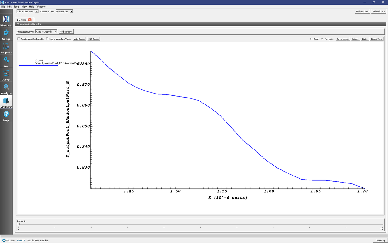
Fig. 300 Visualization of the S-parameters vs wavelength.
To view the pulse propagating down the waveguide proceed as follows:
Select Data Overview from the Add a Data View drop-down.
Expand the Scalar Data tree and the E tree.
Select E_z to view the z-component of the E field.
Make sure that Clip Plot is selected to clip the data to show the field pattern inside the waveguide.
To fix the color scale, set the Set Minimum and Set Maximum options to -3e-6 and 3e-6, respectively
Now expand the invEps tree and select invEps_y.
Check Clip Plot.
Move the Opacity slider to view the E field and invEps field data together.
Further Experiments
This example can be easily modified to use different materials and/or different dimensions and slope angles. Try changing the slope angle or the waveguide dimensions or the materials to fit your needs.
Additional simulations can be run in order to study the effect of the slope angle and the waveguide dimensions on the transmission of the signal. Using the h5py python library, further post processing can be done in order to combine and plot the results of multiple runs. Below are some results that show the effect of the slope angle and the waveguide width on the transmission of the signal.
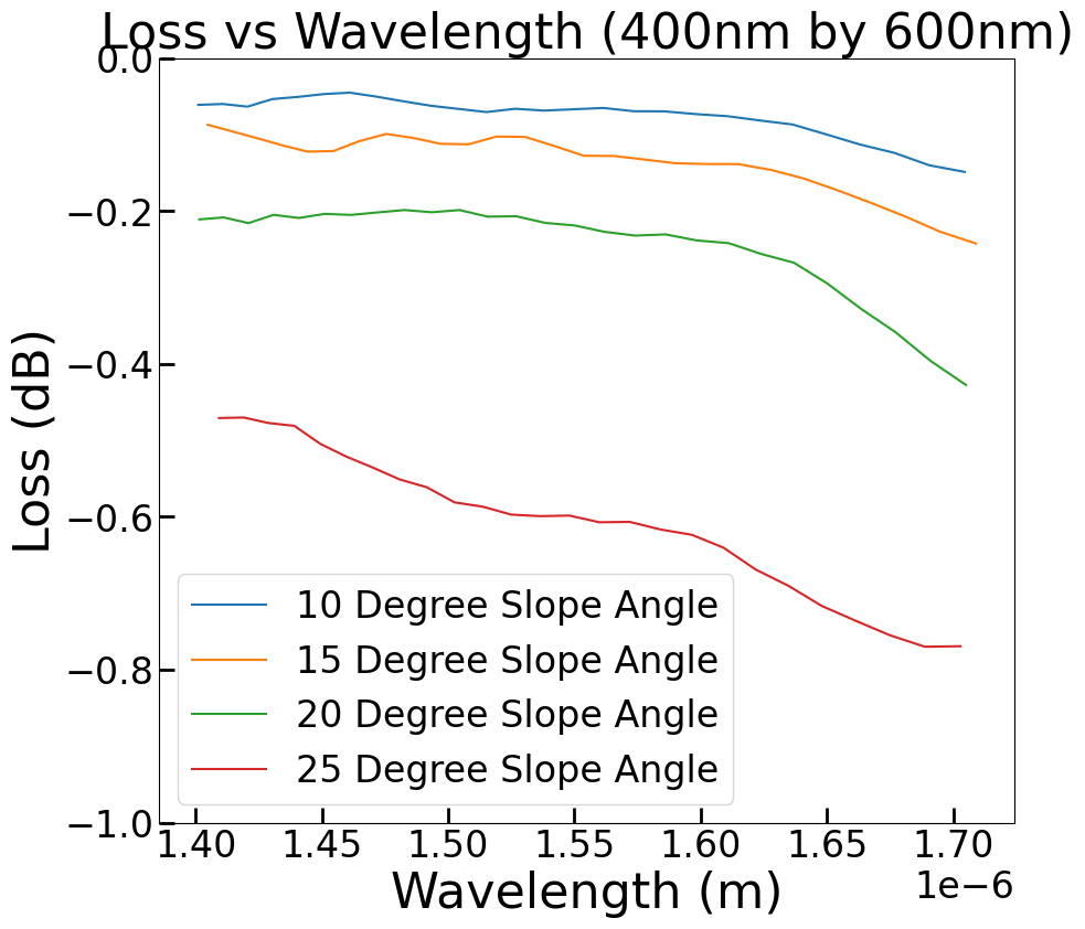
Fig. 301 Visualization of the insertion loss vs wavelength with waveguide dimensions of 400nm by 600nm.
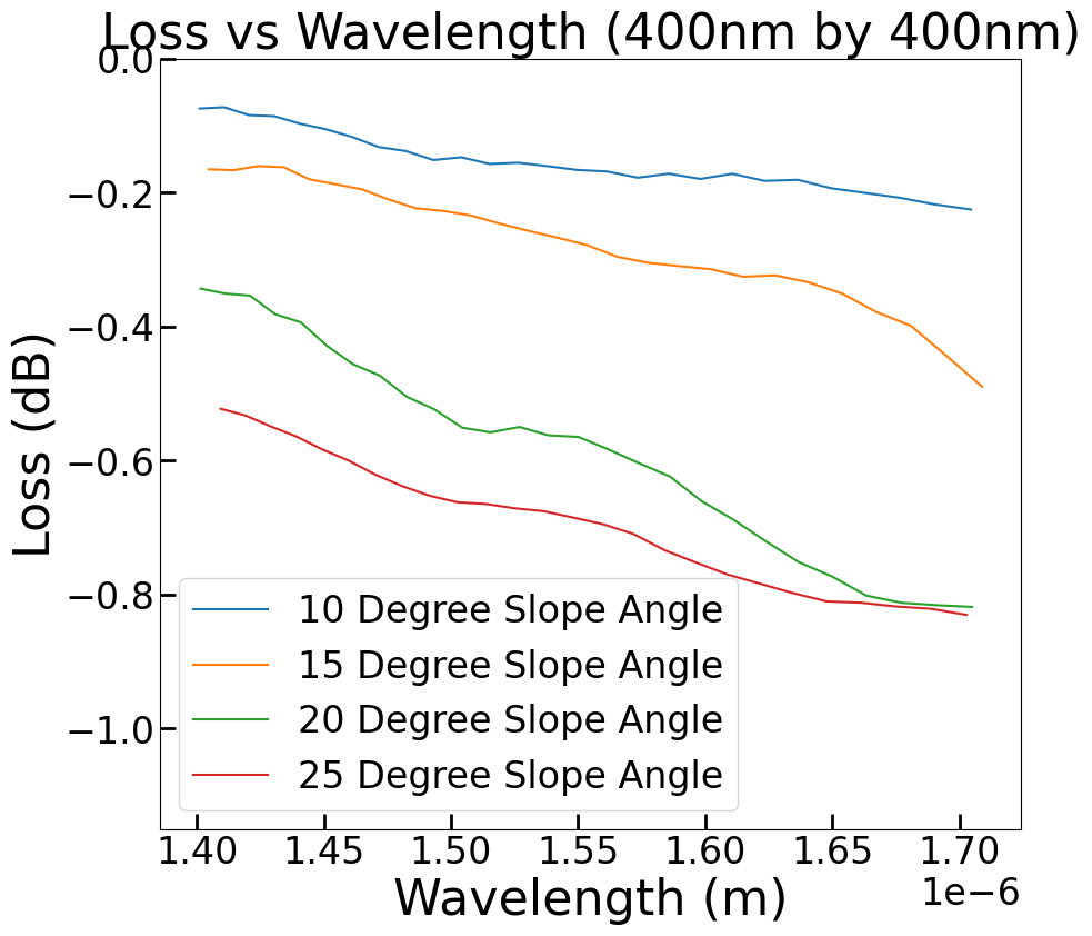
Fig. 302 Visualization of the insertion loss vs wavelength with waveguide dimensions of 400nm by 400nm.
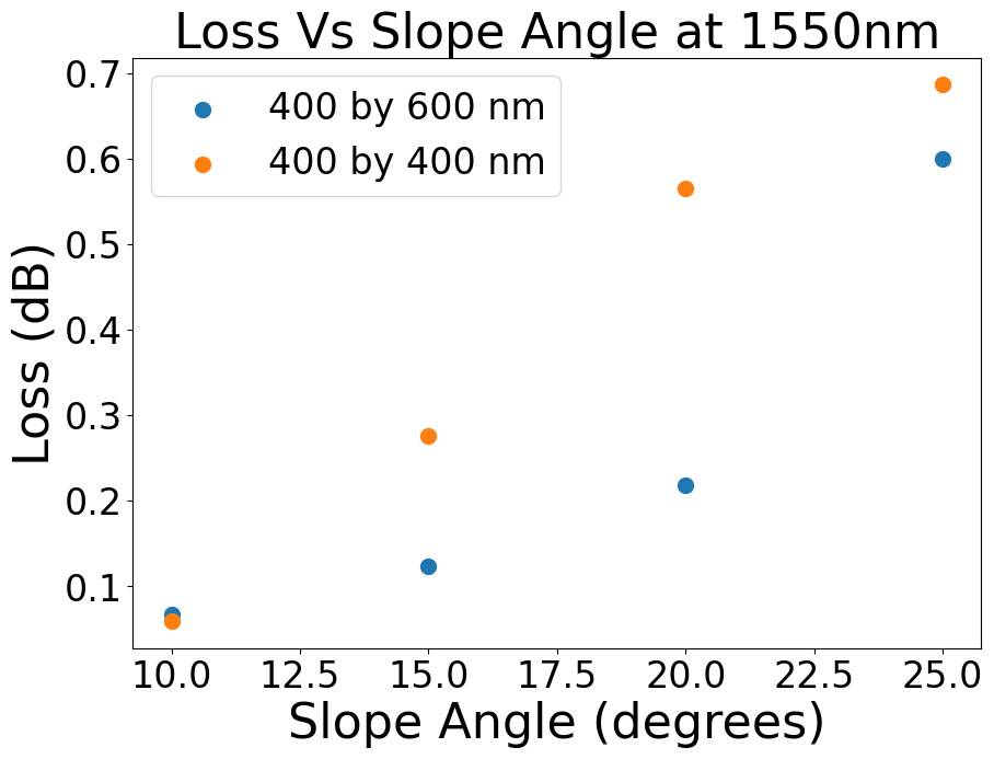
Fig. 303 Visualization of the insertion loss vs slope angle with at 1550nm wavelength.