Dielectric Waveguide With Roughness (dielectricWaveguideModeCalcRough.sdf)
Keywords:
- Photonic Waveguide, Guided Mode
Problem Description
This example demonstrates how to add roughness to a waveguide and how to implement a variable grid to resolve roughness that would otherwise be too computationaly expensive to resolve. Since roughness features of a waveguide are typically on the order of nanometers, a very high resolution (and therefore small cell size) is required. By using a variable grid, a user is able to increase the resolution where needed and decrease the resolution elsewhere to maintain the computational efficiency of a uniform grid.
Opening the Simulation
To open this example open an instance of XSimComposer and follow the steps below:
Select the New → From Example… menu item in the File menu.
In the resulting Examples window expand the XSim for Electromagnetics option.
Expand the Photonics option.
Select Dielectric Waveguide With Roughness and press the Choose button.
In the resulting dialog, create a New Folder if desired, and press the Save button to create a copy of this example.
Simulation Variables
This example contains a number of variables defined to make the simulation easily modifiable.
EPS_SILICON and EPS_SILICA: Relative permittivities of silicon and silica. These constants are used in multiple parameters and in the accompanying Python file for solving the waveguide mode.
WAVELENGTH_CENTER: Center wavelength of the input signal. This wavelength is also used for the calculation of the fundamental guided mode of the device.
DY_REFINED: The cell size desired within the refinement region.
USE_DY_REFINED: A switch that when set to 1 will replace DY with DY_REFINED in calculations such as the CFL time step. By default this is set to 0.
The Materials section contains just silicon and silica. The Geometries section includes the GDS waveguide. In Field Dynamics, there are FieldBoundaryConditions and CurrentDistributions to be aware of. In photonics simulations, Matched Absorbing Layers (MALs) are the most stable boundary conditions for preventing reflections. This simulation makes use of XSim’s Wave Launcher to launch a unidirectional wave down the waveguide with a mode defined by the file generated by the computeWaveguideModes.py analyzer.
Setting up the Roughness
As delivered, this example comes equipped with a geometry imported from a GDS file. For more on importing a geometry from a GDS file, see the Y Splitter example documentation. At the moment roughness is only supported on geometries made from importing a GDS. To add roughness to the waveguide, proceed as follows:
Expand the geometry object in the Geometries section by clicking on the + symbol next to waveguideGeom.
Select the Boundary0 object under waveguideGeom.
- Switch the roughness type option from roughnessDisabled to stochasticODE. Fill in the following parameters under stochasticODE as follows:
RMS amplitude: 50e-9
normal tolerance: 45
Ramp-up distance: 0.0
Ramp-down distance: 0.0
ODE Correlation: 1000e-9
ODE step size: 140e-9
Random seed: 12345679
export to CSV:
The geometry in the 3D visualization view should look like:
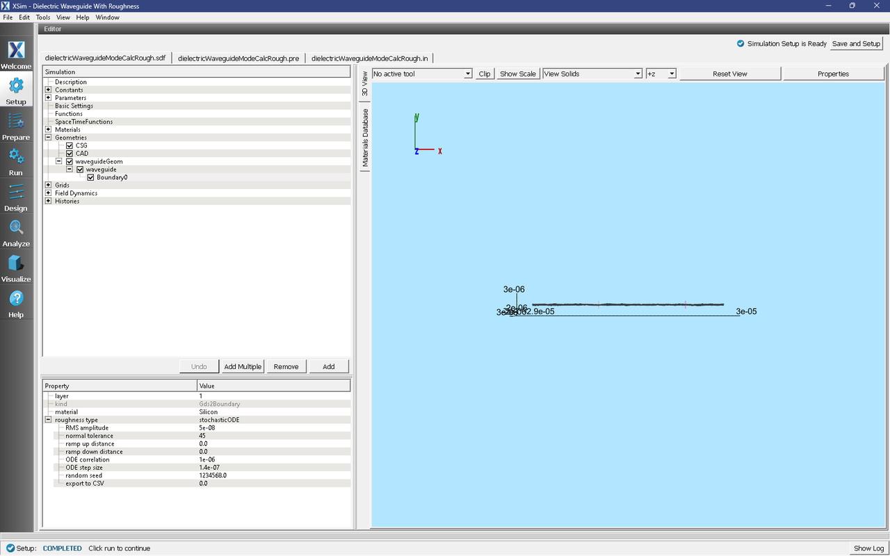
Fig. 253 The waveguide with roughness added to the upper and lower walls in the y direction.
Running the Uniform Grid Simulation
After performing the above actions, continue as follows:
Proceed to the Run Window by pressing the Run button in the left column of buttons. If you changed something in the setup, you will be asked to Save. Click Save upon the request to save.
In the left pane : * Set Number of Steps to 12500. * Set Dump Periodicity to 1250. * Check Dump at Time Zero.
Click on the Run button in the upper left corner of the right pane.
You will see the output of the run in the right pane. The run has completed when you see the output, “Engine completed successfully”. This result is shown in Fig. 254.
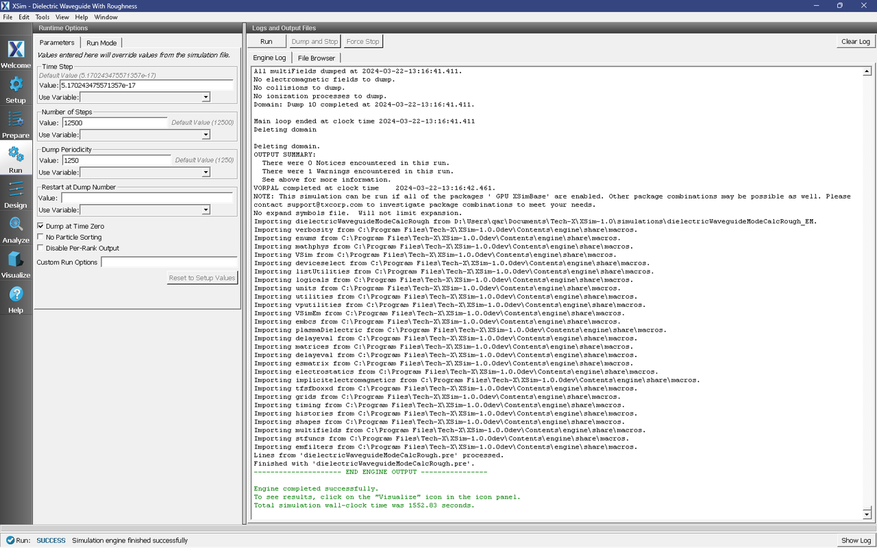
Fig. 254 Running the full simulation.
Visualizing the Uniform Grid Results
After performing the above actions, continue as follows:
Proceed to the Visualize Window by pressing the Visualize button in the left column of buttons.
You may need to Reload Data (bottom left). Visualize the electric field and a cross section of the geometry by following these steps:
From the Add a Data View dropdown, select Data Overview.
Expand Scalar Data, expand E, and select E_y.
Click Clip plot, then Plane Controls, then select Plane3, and enter 1 for the Z Normal
Expand Geometries and select waveguideDualTriangles.
Click Clip plot, then Plane Controls, then select Plane3, and enter 1 for the Z Normal
The resulting visualization pane should look like Fig. 255.
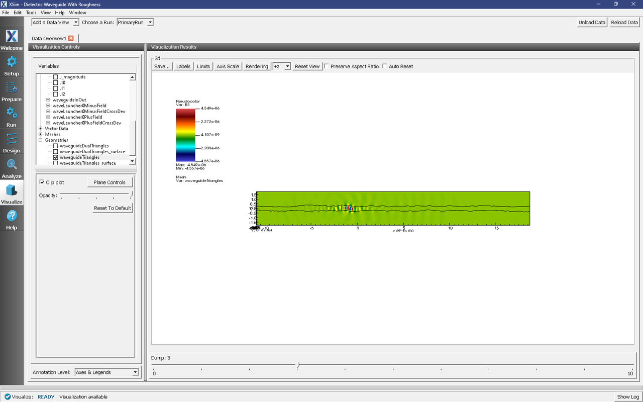
Fig. 255 The visualization pane showing the y component of the E field with the geometry on top.
Slide the dump selector at the bottom of the window to the right to watch the wave travel down the waveguide. It is clear that with this level of roughness that the transmission of the wave will not be great.
Setting Up the Variable Grid
In XSim, a variable grid is implemented into the simulation by adding in a Refinement Region. This is a 3D box in which the cell sizes inside can be changed to increase the resolution in one or multiple directions. The refinement region will then take the total number of cells in each direction and will automatically adjust the size of the cells outside of the refinement region to smoothly fit in the rest of the cells into the domain. In this simulation, the resolution in y is increased. In this example, a refinement region has already been created and is inactive. To activate this refinement region, proceed as follows:
Expand the Grids and Grid sections.
Right click on refinementRegion0 and click Activate.
This refinement region was created by performing the follwing actions:
Expand the Grids section and right click on Grid.
Select Create Refinement Region.
A new option will appear under Grid called refinementRegion0. To make the box surround the waveguide and increase the resolution in y, fill in the following options in the refinement region as follows:
xMin: GRID_X_BGN
xMax: GRID_X_END
cellSizeX: DX
yMin: -3.5e-7
yMax: 3.5e-7
cellSizeY: DY
zMin: -2e-7
zMax: 2e-7
cellSizeZ: DZ
Now to change the resolution in the y direction, expand the Parameters section and select USE_DY_REFINED. Set this parameter equal to 1. This parameter acts as a switch that will replace DY with a smaller value specified by DY_REFINED in all calculations. Since the grid has changed, a new mode file needs to be calculated. Expand the Field Dynamics section and under CurrentDistributions, deactivate waveguideModeLauncher0 by right clicking on it and select Deactivate. Next, expand the Geometries tab and expand the waveguideGeom geometry. Select Boundary0 and set roughness type to “roughnessDisabled”. Save the simulation and continue to the run tab. Now to generate the necessary data to recalculate the fundamental mode of the waveguide, proceed as follows:
Click on the Reset to Setup Values button.
Set the Number of Steps and Dump Periodicity to 1.
Make sure that Dump at Time Zero is selected.
Click Run.
Upon successful completion of the engine, proceed to the next section.
Solving for the Eigenmode
After performing the above actions, continue as follows:
Proceed to the Analyze Window by clicking the Analyze button on the left.
Select computeWaveguideModes.py and click Open under the list.
Update the analyzer fields accordingly by choosing the corresponding variables under Use Variable :
simulationName: dielectricWaveguideModeCalcRough
datasetName: invEps
transverseSliceX: PORT_X_INPUT
transverseSliceLY: PORT_YBGN
transverseSliceUY: PORT_YEND
transverseSliceLZ: PORT_ZBGN
transverseSliceUZ: PORT_ZEND
vacWavelength: 1.55e-6
nModes: 1
writeFieldProfile: D
modeFileName: port1
Normalize: checked
compMajorC: checked
Overwrite: checked
Click Analyze in the top right corner.
The analyzer will only find guided modes. The results should resemble Fig. 256. We see that the analyzer found the fundamental mode and gives the effective index of the mode under Neff. This parameter is necessary for using the Wave Launcher to launch a unidirectional wave. This value is saved as a constant as NEFF_FROM_ANALYZER.
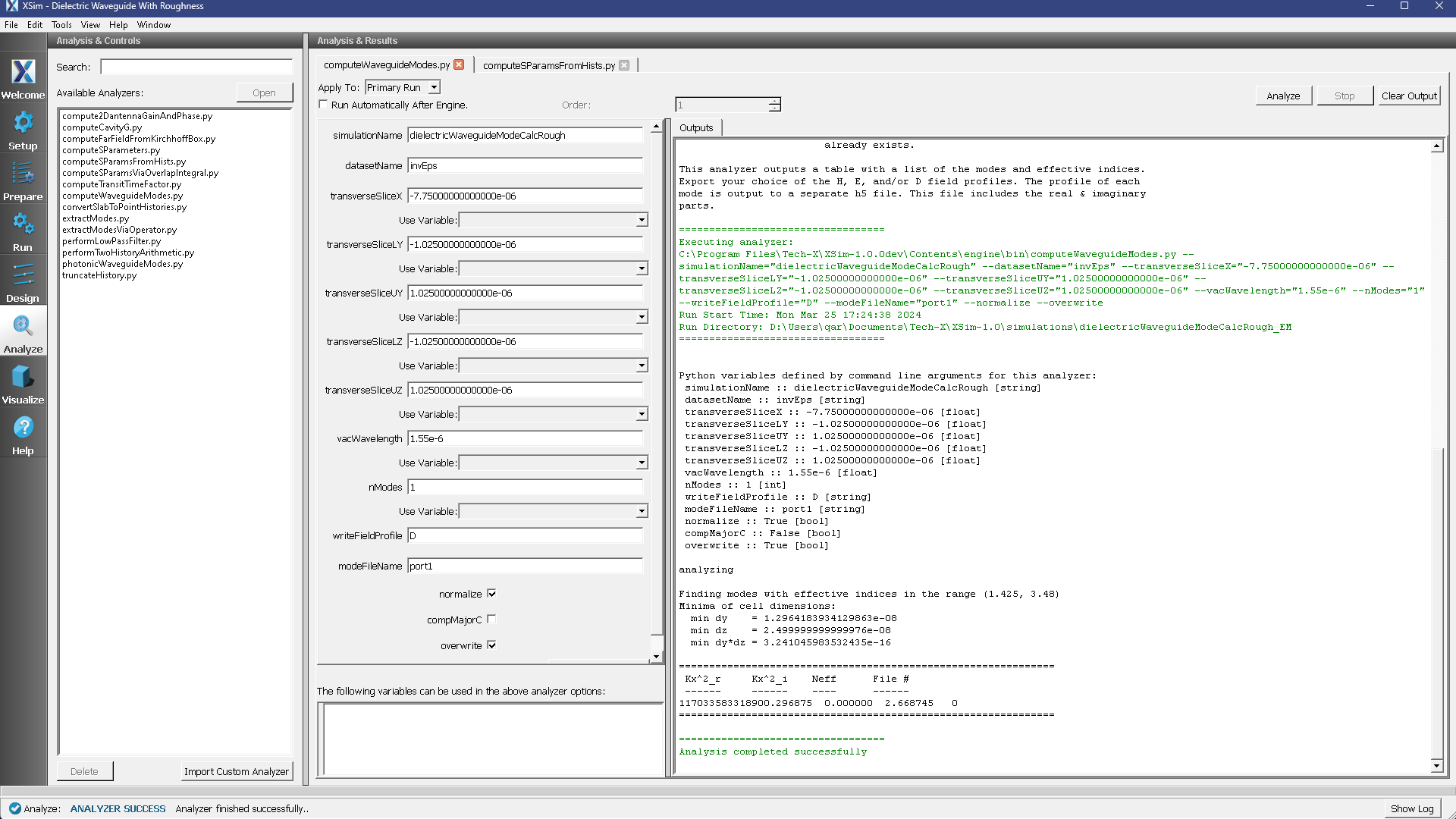
Fig. 256 The analyzer window after a successful run of computeWaveguideModes.py.
Setting up the Variable Grid Simulation
After performing the above actions, continue as follows:
Proceed to the Setup Window by pressing the Setup button in the left column of buttons.
Activate the wave launcher.
Expand Field Dynamics.
Expand CurrentDistributions.
Right Click on waveguideModeLauncher0.
Left click on Activate.
Click on Save and setup in the top right corner.
From the setup tab we will now add in roughness that can be resolved with the variable grid. Add in roughness the same way as before but change the RMS amplitude to 10 nm.
Running the Variable Grid Simulation
To run the variable grid simulation, proceed as follows:
Proceed to the Run Window by pressing the Run button in the left column of buttons. You will be asked to Save. Click Save upon the request to save.
In the left pane, click on Reset to Setup Values to run the full simulation which launches this wave down the waveguide.
Check Dump at Time Zero.
Make sure that Number of Steps is set to 24000.
Make sure that Dump Periodicity is set to 2400.
Click on the Run button in the upper left corner of the right pane.
You will see the output of the run in the right pane. The run has completed when you see the output, “Engine completed successfully.”
Analyzing the Results
When designing a waveguide and simulating the roughness, one might be interested in calculating the S parameters and spectral power of the wave traveling down the waveguide. XSim features an analyzer that will compute both of these quantities.
After visualizing the data and making sure the simulation is behaving as expected, proceed to the Analyze Window.
Click on the computeSParamsFromHists.py analyzer to open it and fill in the necessary parameters as follows:
simulationName dielectricWaveguideModeCalcRough
firstStep: 0
lastStep: 12500 (or 24000 for variable grid simulation)
stepOffset: 0
maxWavelength: WAVELENGTH_MAX
minWavelength: WAVELENGTH_MIN
inDirection: 0
inSlabE: slab0_E
inSlabB: slab0_B
inSign: 1
outDirection: 0
outSlabE: slab1_E
outSlabB: slab1_B
outSign: 1
timeSample: 10
cellSamples: 1:1:1
outputFileName : blank
outputSuffix: blank
overwrite: checked
Click Analyze in the top right corner.
The results should resemble Fig. 257
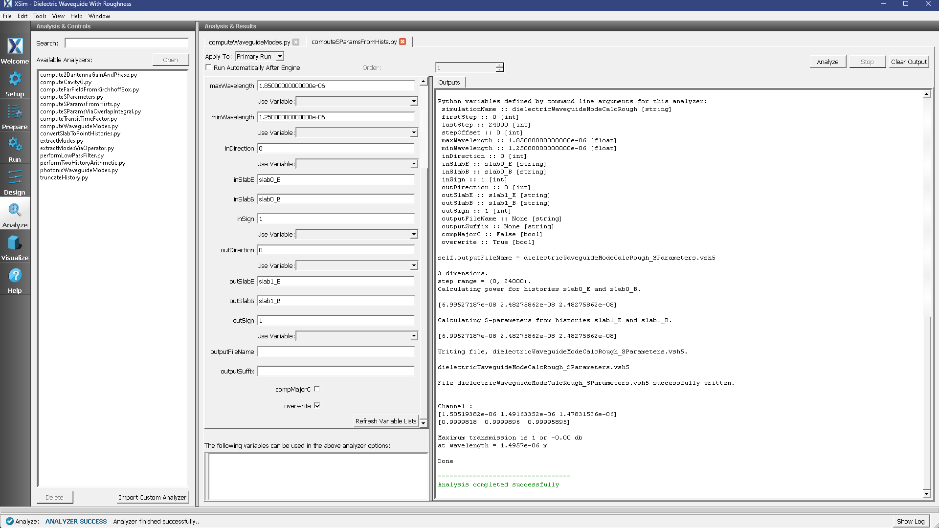
Fig. 257 The analyzer window after a successful run of computeSParamsFromHists.py.
Upon successful completion of the analyzer, proceed to the Visualize tab.
From here, click on the drop down menu called Add a Data View and select 1-D Fields.
To visualize the S-parameters and the input power:
Click Add Curve
Select S_slab1_EAndslab1_B
Click Apply, followed by Ok.
Click on the Add Window button and repeat the same process as before but this time select slab0_EAndslab0_BPower from the drop down menu.
The resulting plots will have the S-parameters per wavelength on top and the spectal input power on the bottom, as in Fig. 258
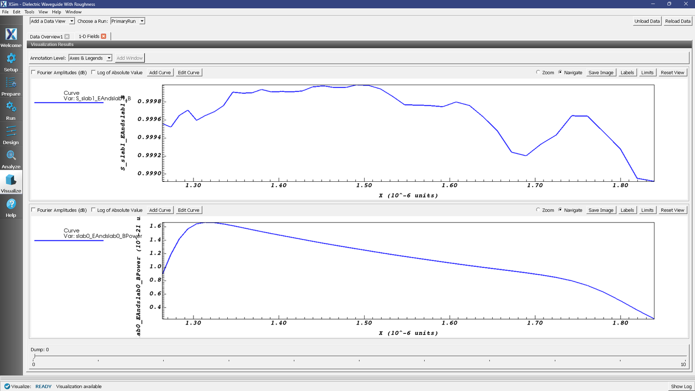
Fig. 258 The visualization window after adding in the plots of the S-parameters and the spectral input power.
Further Experiments
Change the DY_REFINED and DX parameters to analyze different roughness amplitudes and correlation distances. Change the variable grid to increase the resolution in the propagation direction and then increase the roughness in this dimension as well.
Running on the Cloud
Often times, roughness with an RMS amplitude of 2nm or smaller is required to be simulated. These simulations can become very large and will require more computational resources. Using Cloudsim, these small roughness simulations can be run with ease using AWS’s “p” instance types with Nvidia V100 GPUs. For simulations with very fine roughness, it is recommened that a p3.x8large instance type is used since this compute node features 4 V100s on a single node. A cluster with a cheap headnode and a single p3.8xlarge compute node is recommnended so that the compute node is charged only when the simulation is being run and the analysis can take place of the cheaper head node. Below are suggestions on setting up the hardware, the performance results of that hardware configuration, and tips for understanding how much the simulations will cost.
Hardware configuration
Head Node : t3.large
Compute Node : p3.8xlarge
Max Number of Compute Nodes : 1
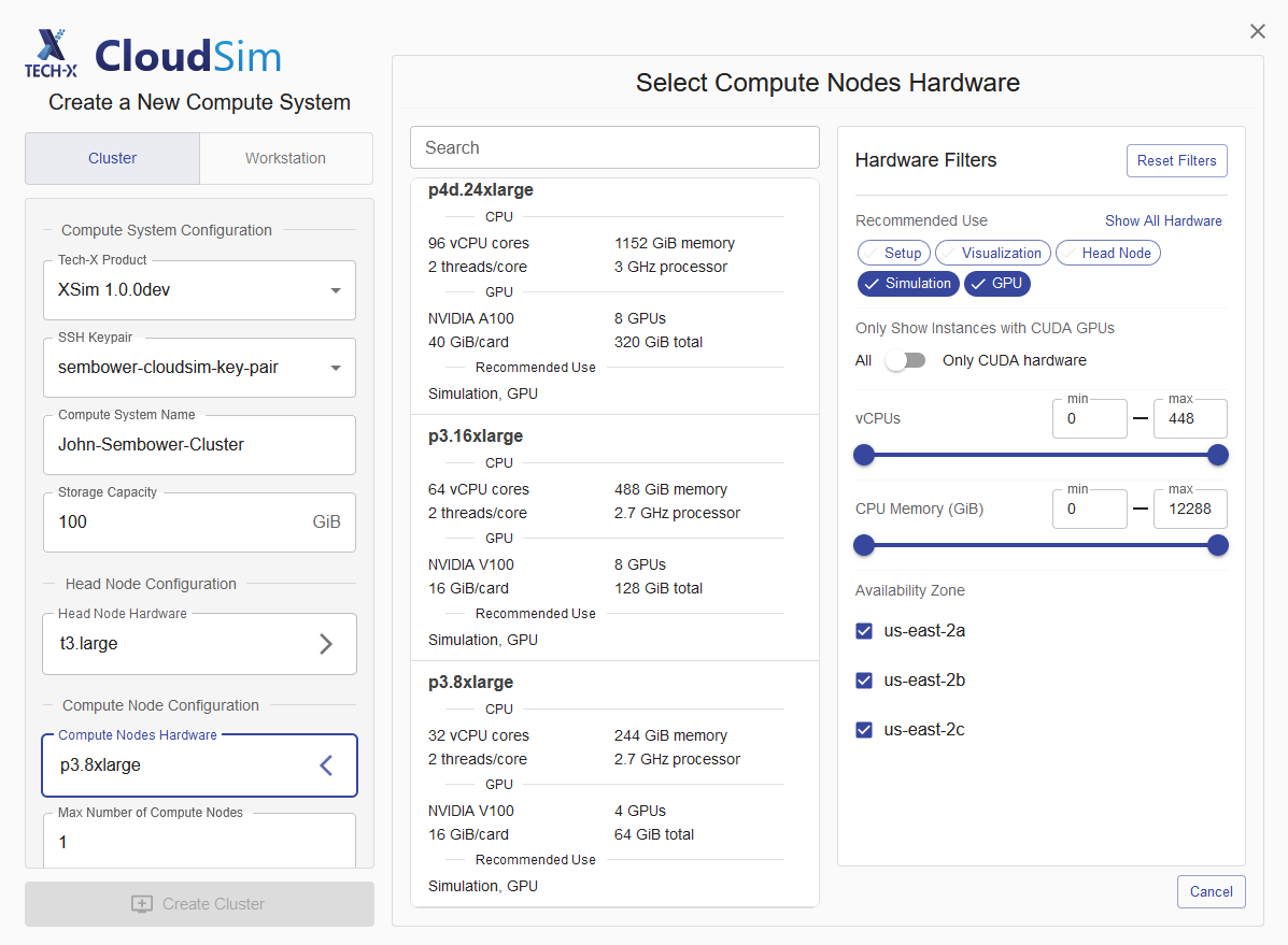
Fig. 259 A view of the cluster creation screen for the recommeneded hardware.
Below are some performance results for 2 problems of different sizes:
Performance Results (Results from 5/2024 when the hourly rate for this instance type was $12.24 an hour for the compute node)
2nm Roughness, 1 Nvidia V100 GPU, 91M cells: 1.4 Gcells/sec.
2nm Roughness, 4 Nvidia V100 GPUs, 273M cells: 4.3 Gcells/sec (1.08 Gcells/GPUsec).
In order to get a sense of how expensive a simulation is to run on a given set of hardware, the following procude is recommeneded:
Start your cluster and note the time.
Start your simulation and note the time when the simulation begins to start taking steps.
Note the time when the simulation concludes.
Stop the instance and note the time.
The above procedure is useful when deciding what hardware types to use based on your simulation needs.