Adiabatic Tapered Splitter (adiabaticSplitter.sdf)
Keywords:
- S Parameter, Mode Launcher, MAL, Guided Mode, Photonic Device
Problem Description
This passive splitter uses adiabatically tapered waveguides to split a pulse of light into two seperate waveguides with minimal scattering and mode-conversion. For this splitter the length of the taper is 40 micrometers, the separation between the input waveguide and the two output waveguides is 300 nanometers, and the waveguide starts with a height of 700 nanometers and is linearly tapered down to 200 nanometers. The device itself is made from a 220 nanometer thick ribbed waveguide with a partial etch distance of 60 nanometers and is made of silicon. Beneath the device is a buried silicon dioxide layer with vaccuum above. The fundamental mode of the waveguide is calculated and launched down the device as a broadband signal. Finally, the S parameters are calculated via an analyzer.
This examples makes use of a “Photonics simulation template” intended to allow for rapid setup of any passive photonic device, provided the ports are aligned with the X-Axis. Matched Absorbing Layers (MALs) are used to dampen the E, B and D fields near the boundary of the simulation.
This simulation can be performed with a XSimEM license.
Opening the Simulation
The Adiabatic Tapered Splitter example is accessed from within XSimComposer by the following actions:
Select the New → From Example… menu item in the File menu.
In the resulting Examples window expand the XSim for Electromagnetics option.
Expand the Photonics option.
Select Adiabatic Tapered Splitter and press the Choose button.
In the resulting dialog, create a New Folder if desired, and press the Save button to create a copy of this example.
All of the properties and values that create the simulation are available in the Setup Window as shown in Fig. 265. You can expand the tree elements and navigate through the various properties. The right pane shows a 3D view of the geometry, as well as the grid, if actively shown. To show or hide the grid, expand the Grid element and select or deselect the box next to Grid.
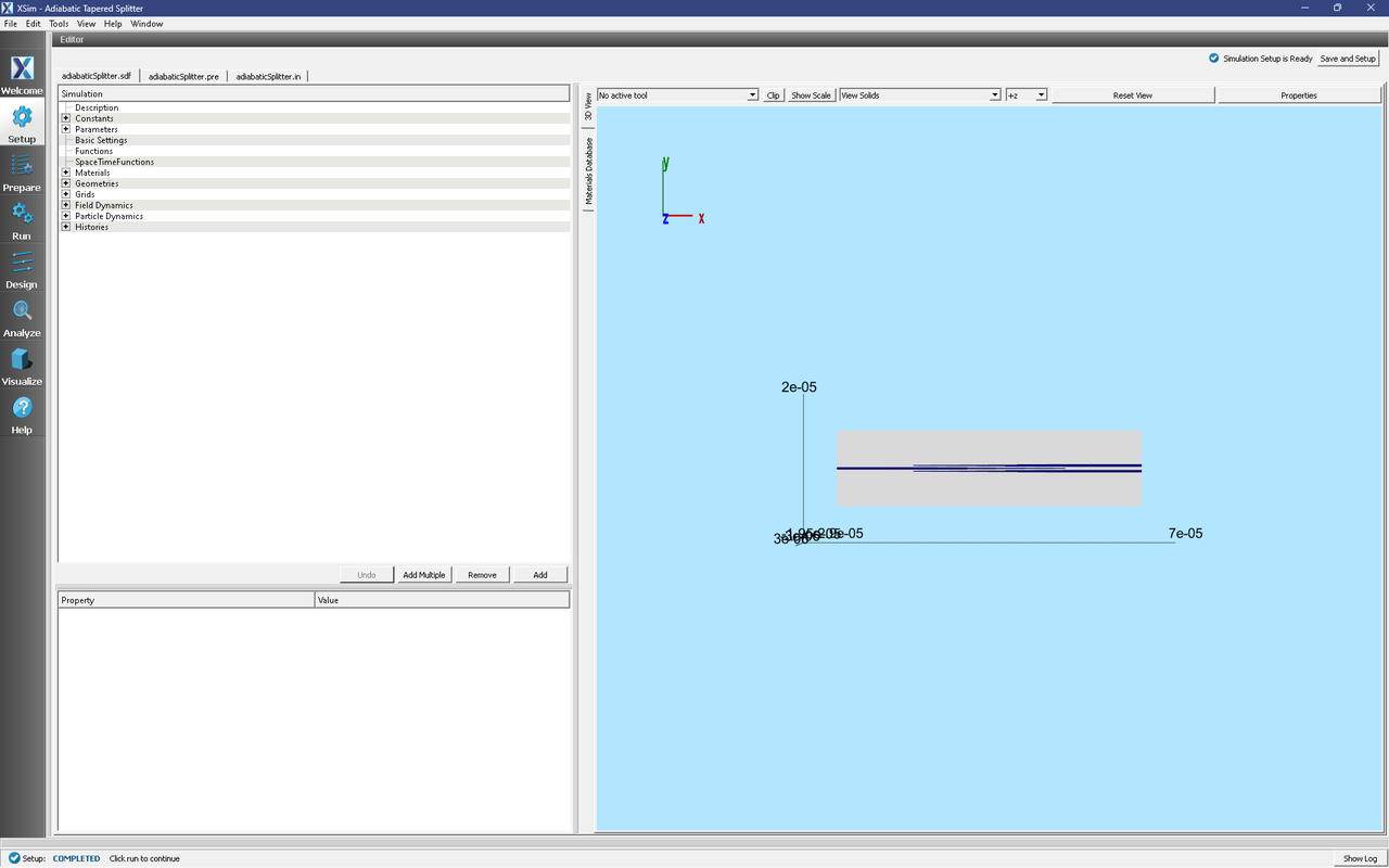
Fig. 265 The Setup window for the Adiabatic Tapered Splitter example showing the imported gds file.
Simulation Properties
This example contains a number of Constants defined to make the simulation easily modifiable.
General Simulation Constants:
WAVELENGTH_CENTER = The central wavelength of the excitation.
WAVELENGTH_MAX = The maximum wavelength of the simulation.
WAVELENGTH_MIN = The minimum wavelength of the simulation.
WAVELENGTH_XMAL/WAVELENGTH_YMAL/WAVELENGTH_ZMAL= The thickness of the MAL’s in the X/Y/Z directions in terms of the central wavelength.
CELLS_PER_WAVELENGTH_CROSSSECTION = The number of cells per central wavelength in the Y and Z direction.
CELLS_PER_WAVELENGTH_AXIAL = The number of cells per central wavelength in the X direction.
This simulation applies a wide frequency band signal to the fundamental spatial mode profile.
The Materials section contains just Silicon and Silica. This section is where one can add or edit materials that get attached to GDS/CSG objects. These Materials contain the relative permittivity.
In Field Dynamics there are FieldBoundaryConditions which set the boundary conditions of the simulation. In photonics simulations, Matched Absorbing Layers (MALs), are the most stable boundary conditions for preventing reflections.
Under Basic Settings you can see that the dielectric solver is set to volume averaging. This feature enables second order accuracy for simulations using dielectrics.
KLayout
The geometry in this simulation was generated using KLayout, a free tool for generating GDS files. In this section, a description of the necessary steps for creating this geometry is provided.
First, download KLayout to your local machine. Here is a link to their download page: https://www.klayout.de/build.html. Once you have successfully installed KLayout, open the application in editor mode and proceed as follows:
Click on File → New Layout.
A pop-up window will appear. Fill in the following inforamtion:
Technology: Leave as is
Top cell: Top (or whatever you prefer)
Database unit: Leave blank
Initial window size: 2 micrometers
Initial layers: 1/0
Create layout in current panel: unchecked
Now you are ready to begin drawing the geometry. Since there are no curved edges in this geometry, all of the shapes will be generated using polygons and boxes. To add in a box, first make sure hat you have a layer selected. Then, proceed as follows:
Select the Box option from the top menu.
Draw a box in the main window by selecting two points. Don’t worry about it being accurate, the exact size can be modified when it is drawn.
Next, click on the Select tool and double click on the box. This will being up a pop-up window with the boxes information.
From this window you can enter the desired coordinates for the lower left and upper right corners of the box.
These boxes are great for making the rectangular extensions of the tapered waveguides that are used for the splitting. To make the tapered waveguides, polygons are used since they allow for the user to define N points. Since the tapered waveguiedes use a linear taper, only 4 points are required. To add a polygon, proceed as follows:
Select the Polygon tool from the menu.
Draw 4 points by clicking on four different locations. On the fourth click, make sure to double click to end the drawing.
Click on the Select tool from the top menu and double click on the polygon.
This will bring up a pop-up window that allows you to define the x,y coordinates for each of the 4 points.
The geometry in this example uses three boxes and three polygons whose dimensions are described in the problem description.
GDSII File Import
The GDS File has already been imported, however this example serves as a good demonstration of how to do so.
It may be imported like any other CAD file, however a second dialog box will appear, shown below.
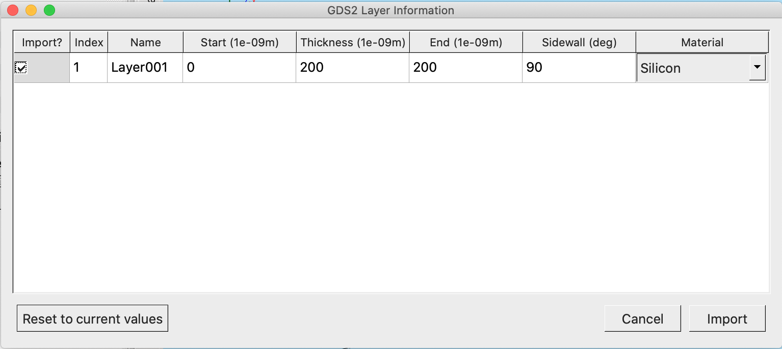
Fig. 266 GDS layer selection.
This allows for selection if the layer should be imported, its starting position on the Z axis, and thickness.
Running the Simulation
When you have saved the setup, continue as follows:
Proceed to the run window by pressing the Run button in the left column of buttons.
Check that you are using these run parameters:
Time Step: 7.544749583079756e-17
Number of Steps: 18000
Dump Periodicity: 1800
Dump at Time Zero: Checked
Click on the Run button in the upper left corner of the right pane.
You will see the output of the run in the right pane. The run has completed when you see the output, “Engine completed successfully”. As seen in Fig. 267.
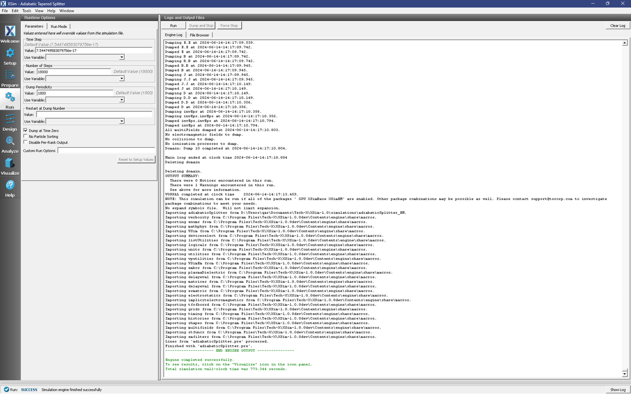
Fig. 267 Run window at completion.
Analyzing the Results
Using post analysis scripts, one can extract the transmission coefficients. This simulation uses 3 “EM Field on Plane” histories (Port1, Port2, Port3) and this data is used to calculate S parameters between these 3 locations using the analysis script computeSParamsFromHists.py.
Follow these steps:
Proceed to the Analyze Window by clicking the Analyze button on the left.
Select computeSParamsFromHists.py and click Open under the list.
Now update the analyzer fields accordingly.
firstStep: 0
lastStep: 18000
stepOffset: 0
maxWavelength: 1650e-9
minWavelength: 1450e-9
inDirection: 0
inSlabE: Port1_E
inSlabB: Port1_B
insign: 1
outDirection: 0
outSlabE: Port2_E (or Port3_E)
outSlabB: Port2_B (or Port3_B)
outSign: 1
The remaining parameter default values will work. Hit the Analyze button in the top right corner. After a successful run the window should resemble Fig. 268.
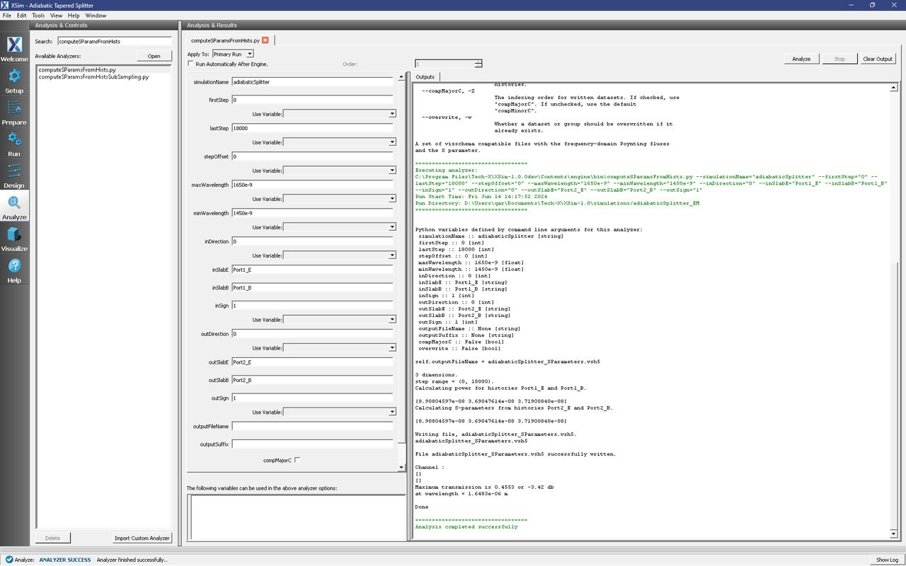
Fig. 268 Analyze window with output from computeSParamsFromHists.py.
Visualizing the results
After performing the above actions proceed to the Visualize Window by pressing the Visualize button in the left column of buttons.
Near the top left corner of the window, select 1-D Fields from the Add a Data View drop-down.
In the Plot Control panel select the S_Port2_EAndPort2_B option for graph 1.
Set the other Graphs to None
The results are shown in Fig. 269. As expected, the S parameters for port 2 show that the power across the spectruc of the excitation is split almost perfectly in half with some loss, as expected.
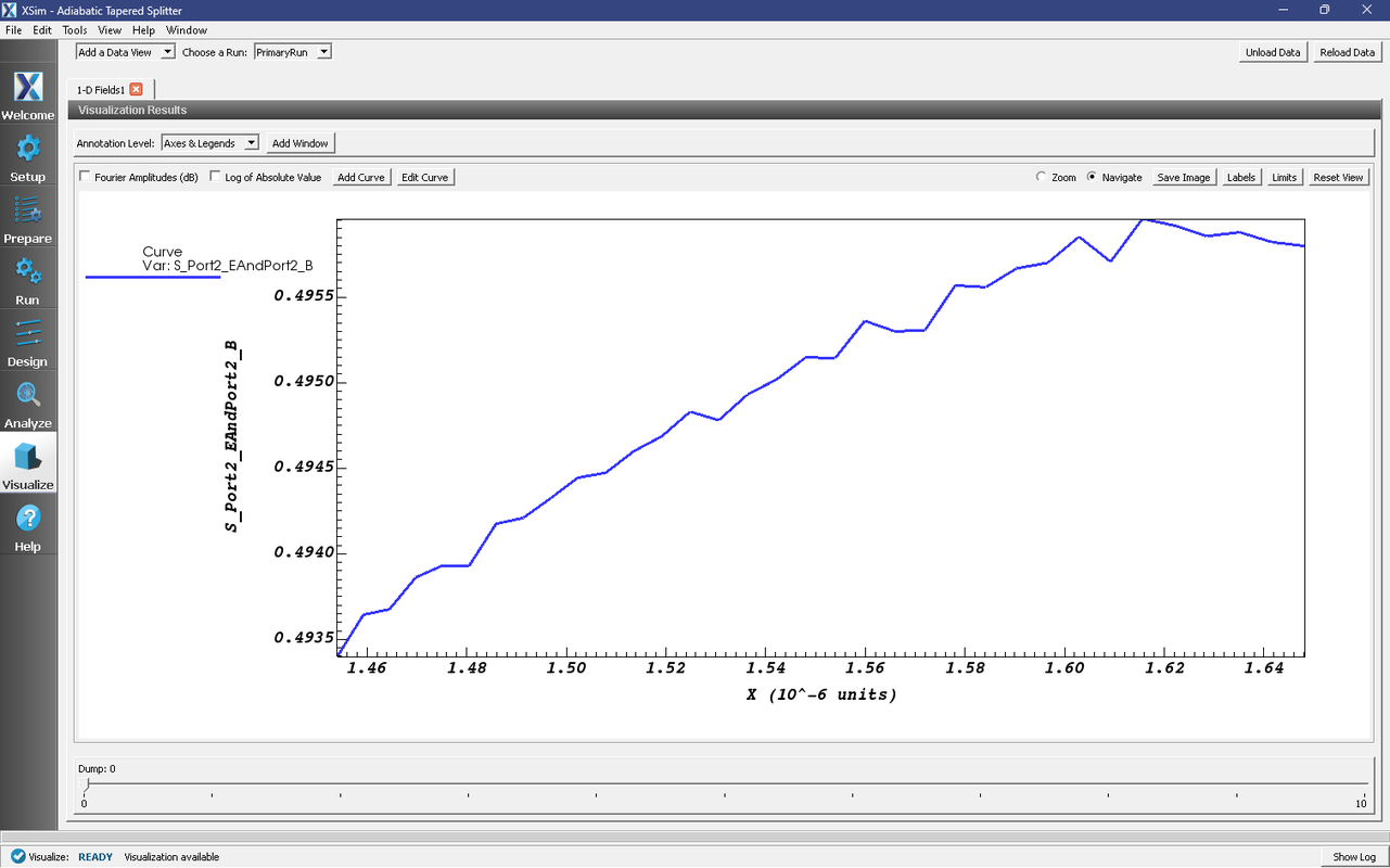
Fig. 269 Visualization of the s-parameters.
Further Experiments
This example can be easily adapted for different GDS files. Use KLayout to create variations of this splitter and calculate the S parameters. Try changing some of the simulation constants.