Dipole Source Illuminating a Photonic Crystal Cavity (photonicCrystalDipoleSrc.sdf)
Keywords:
- dipole source, photonic crystal, transmission efficiency
Problem description
This example illustrates how to model a dipole source that is illuminating cavities inside a hexagonal photonic crystal lattice. The physical arrangement is shown in Fig. 281 and Fig. 282.
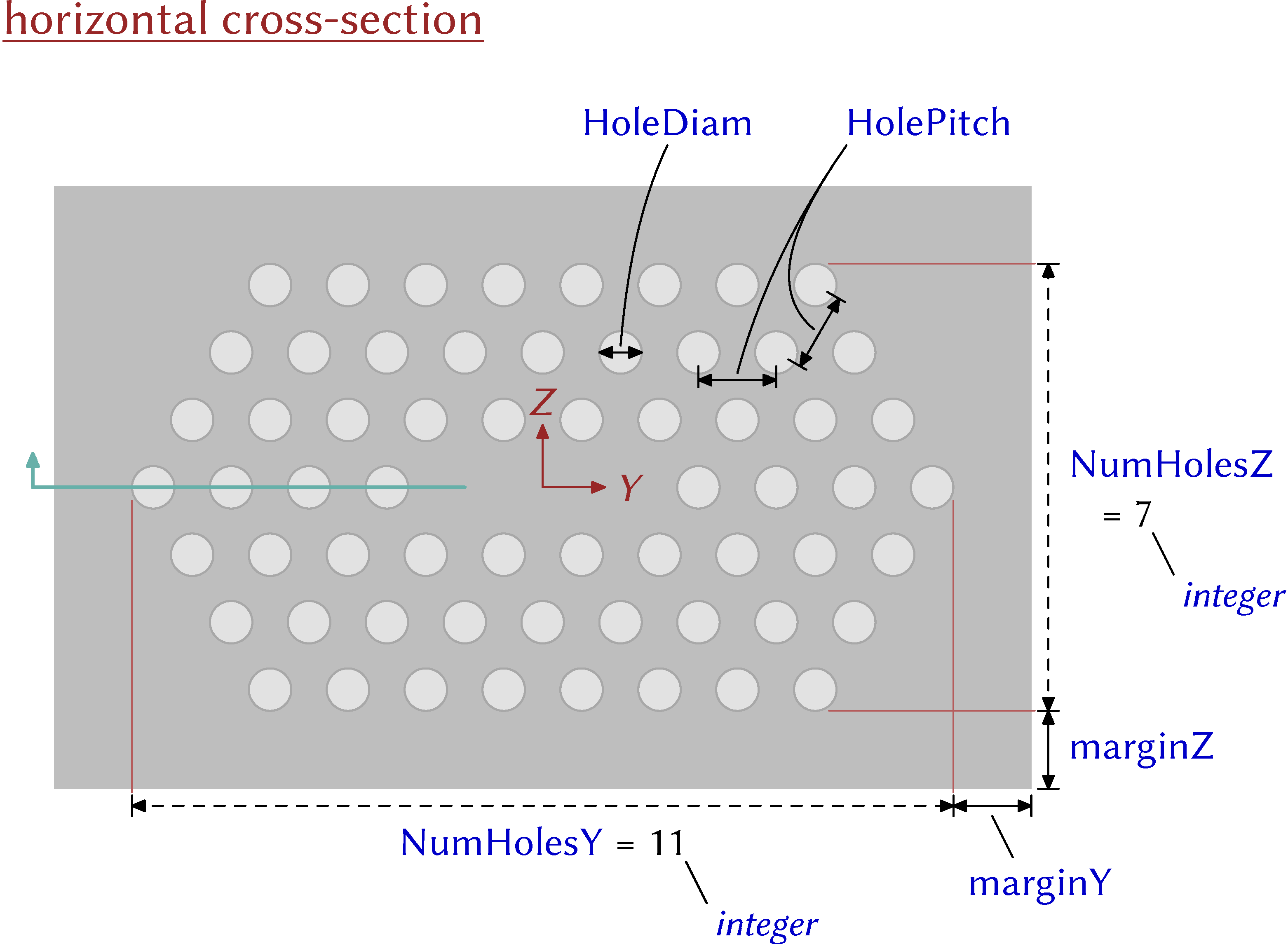
Fig. 281 Top view of photonic lattice.
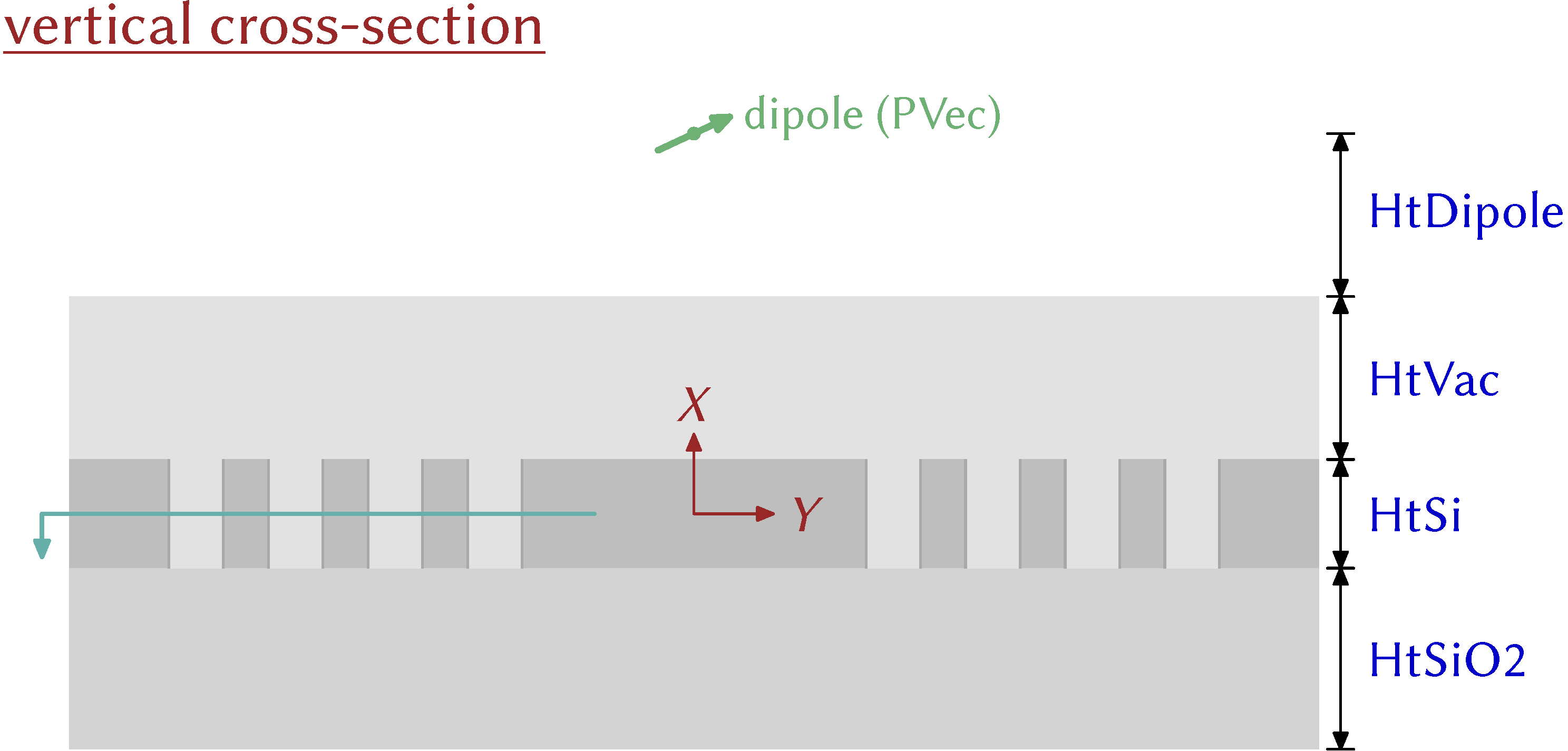
Fig. 282 Side view of photonic lattice.
A point-like dipole lies above the simulation domain, which comprises three layers: a vacuum region above and a solid dielectric below, which together sandwich a central dielectric layer that contains a lattice of holes. This example includes two possible time signals with which to ring the dipole source, as shown in Fig. 283.
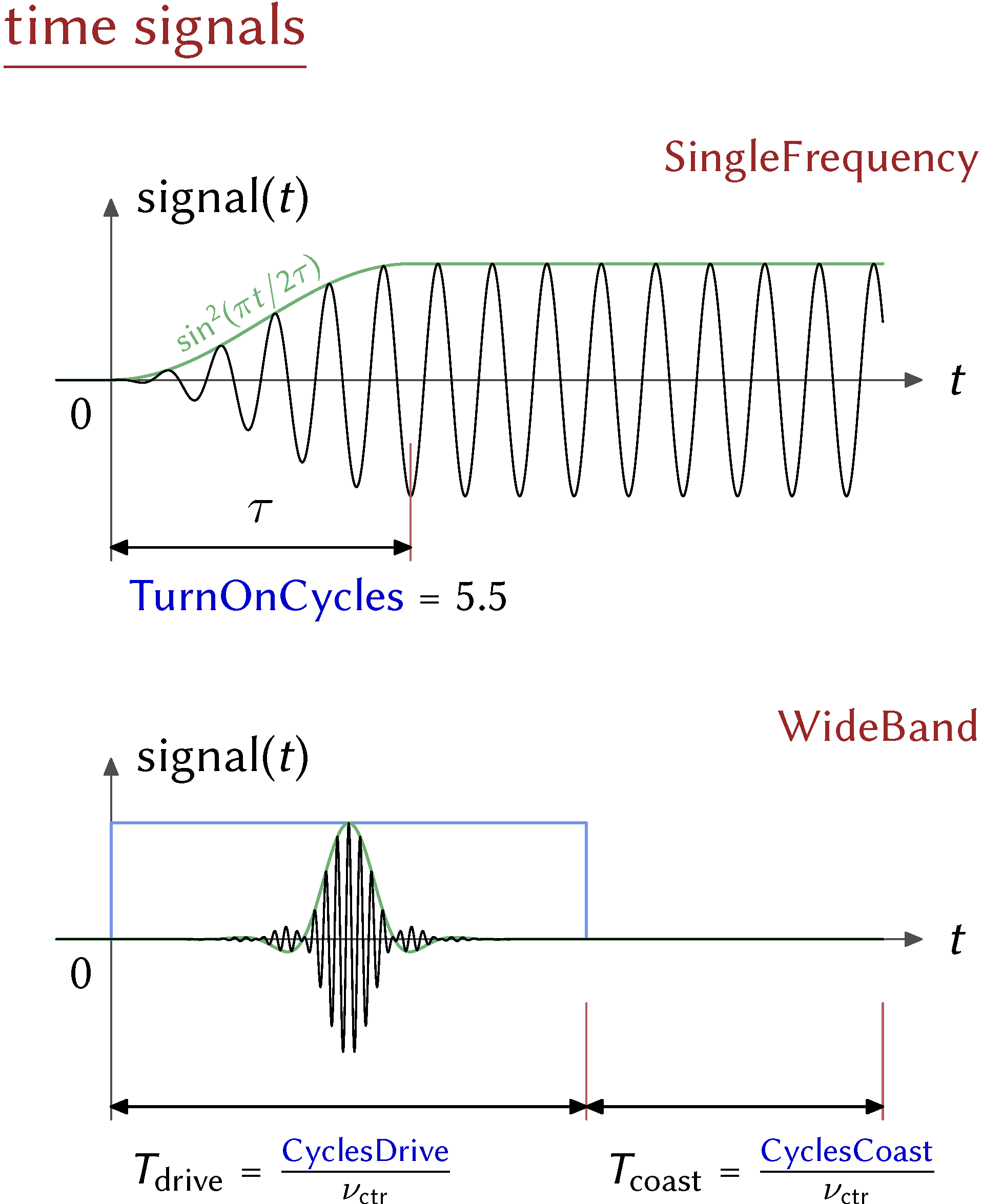
Fig. 283 Two possible time signals for ringing the dipole source.
This simulation can be performed with a VSimEM license.
Opening the Simulation
This Photonic Crystal example is accessed from within VSimComposer through the following steps:
Select the New → From Example… menu item in the File menu.
In the resulting Examples window, expand the VSim for Electromagnetics option.
Expand the Photonics option.
Select “Dipole Source Illuminating a Photonic Crystal Cavity” and press the Choose button.
In the resulting dialog, create a new folder if desired, and press the Save button to create a copy of this example.
All of the properties and values that create the simulation are now available
in the Setup Window as shown in Fig. 284.
You can expand the tree elements and navigate through the various properties,
making any changes you desire. The right pane shows a 3D view of the photonic
crystal geometry. To show or hide the grid, expand the Grid element and select
or deselect the box next to Grid.
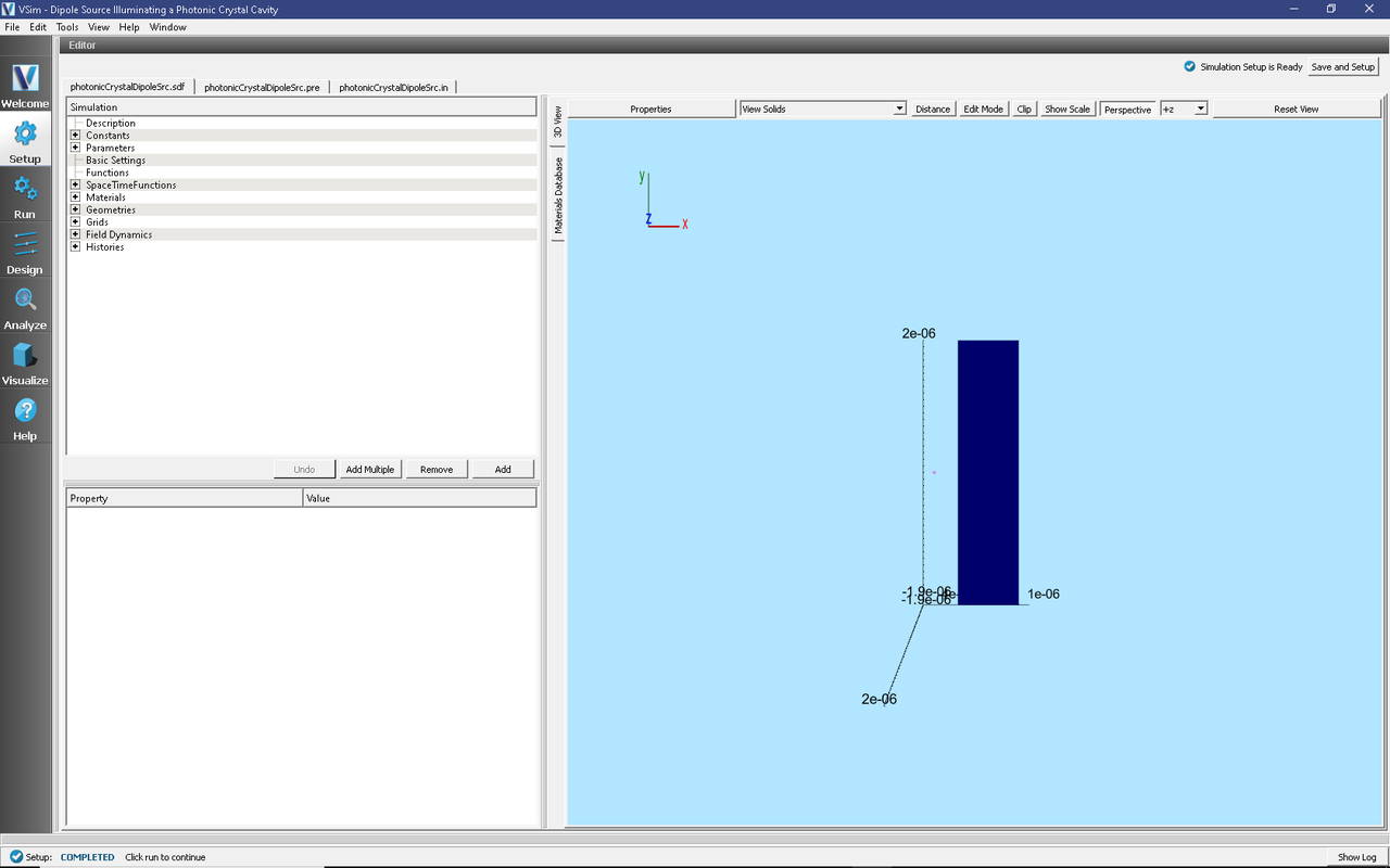
Fig. 284 The Setup Window for the Dipole Source Illuminating a Photonic Crystal Cavity example
Simulation Properties
This example contains a number of constants defined to make the simulation easily modifiable, as can be seen in Fig. 285.
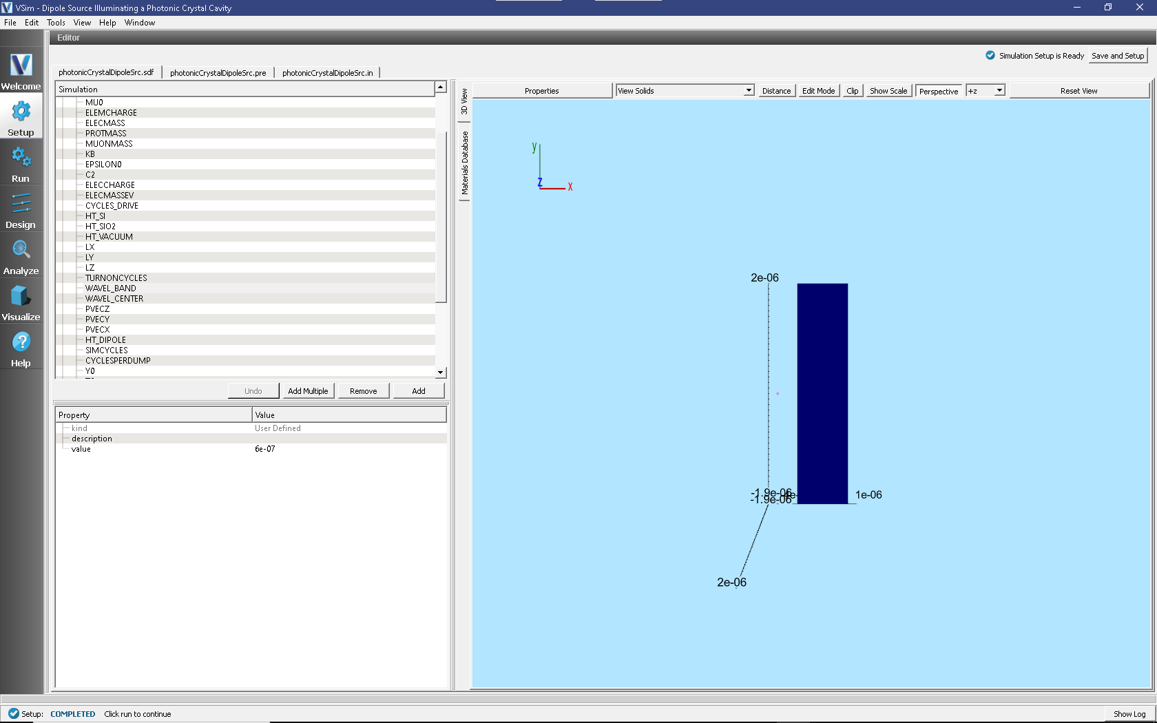
Fig. 285 The Setup Window showing the constants
The following constants should be the only properties you should need to alter in order to specify your simulation domain.
- General Simulation Parameters:
CYCLES_DRIVE= How many cycles at which the E/M source is driven.HT_{VACUUM,SI,SI02}= The height of the vacuum, SI and SI02 layers of the photonic crystal.L{X,Y,Z}= The length of your simulation domain in the {X,Y,Z} dimension.
- Source Specifications: (located in the Parameters section of the Elements Tree)
TURNONCYCLES= The number of cycles you want your single frequency to reach full power.WAVEL_BAND= The wavelength width of your wideband signal, if doing a wideband simulation.WAVEL_CENTER= The central wavelength of your wideband signal, and is the frequency used in the single frequency simulation type.PVEC{X,Y,Z}= The {x,y,z} component of your moment vector for your dipole source.HT_DIPOLE= The height of the dipole from the lowerX boundary.SIMCYCLES= Number of wave cycles you want your simulation to run.CYCLESPERDUMP= Number of cycles between each dump in the simulation.
The tool used to input the wave into the simulation is a port launcher. It specifies the Electric Displacement Field (D) at a boundary in this case the lower X boundary. The functions defining the D on the boundary are defined in the SpaceTimeFunctions element of the Elements Tree.
- SpaceTimeFunctions:
dSingleFreqDipole{Y,Z}= This is the {x,y,z} component of the single frequency dipole source; as seen in Fig. 286, you put this as a parameter in the PortLauncher.dWideBandDipole{Y,Z}= This is the {x,y,z} component of the wideband dipole source; as seen in Fig. 286, you put this as a parameter in the PortLauncher.
To choose which signal you want to input into this example simulation:
Expand the FieldBoundaryConditions tab.
Left click on the portLauncherLowerX condition.
At this point, you should see what is shown in Fig. 286:
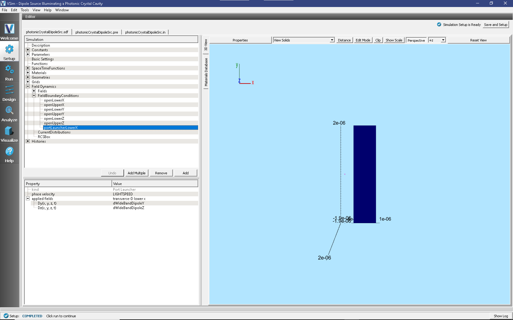
Fig. 286 The Setup Window showing where to specifying the applied field signal for the port launcher
To change the signal applied to the portLauncherLowerX, right click on the Dx(x, y, z, t) or Dy(x, y, z, t) property and select Assign SpaceTimeFunction. This will expand another menu that will show you all four defined SpaceTimeFunctions. Select which one you want to input into your simulation. For this documentation,
dWideBandDipole{Y,Z}is selected by default to demonstrate the functionality of the example.
Running the Simulation
Once finished with the problem setup, continue as follows:
Proceed to the Run Window by pressing the Run button in the left column of buttons.
One can enable MPI options to utilize multi-core systems.
The default values of
Number of Time StepsandDump Periodicityare taken from the parametersSTEPSTOTALandSTEPSPERDUMP, which use the constantsSIMCYCLESandCYCLESPERDUMP. The formulae for these variables can be found back in the Setup Window. These variables are for convenience to calculate good default values and it is important to know that the override option default values ultimately come directly from the numbers in the Basic Settings section.Number of Steps =
STEPSTOTAL= 36250Dump Periodicity =
STEPSPERDUMP= 3600
To run the file, click on the Run button in the upper left corner of the Logs and Output Files pane. You will see the output of the run in that pane. The run has completed when you see the output, “Engine completed successfully.” This is shown in Fig. 287.
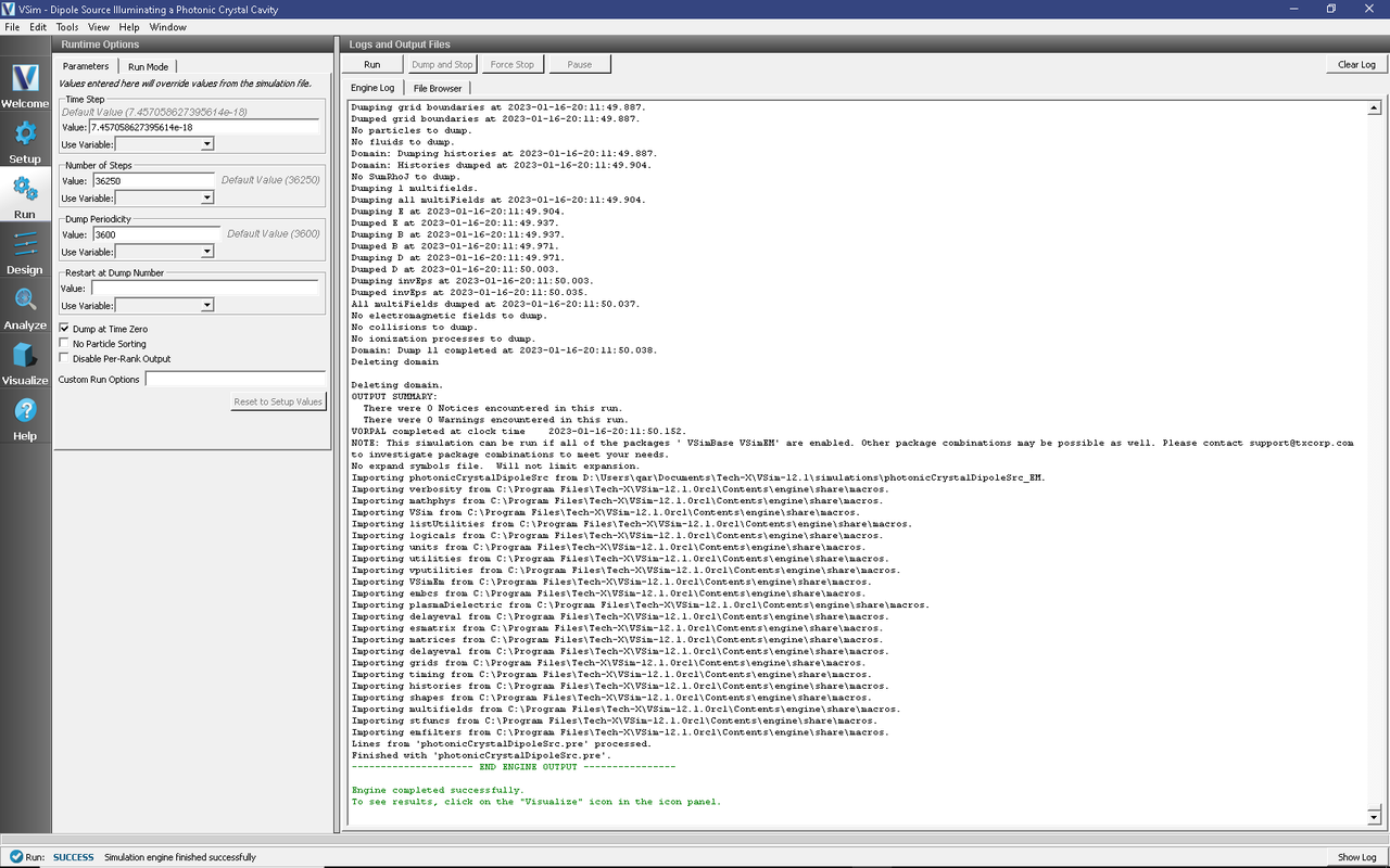
Fig. 287 The Run Window for the Dipole Source Illuminating a Photonic Crystal Cavity example
Visualizing the results
After performing the above actions, continue as follows:
Proceed to the Visualize Window by pressing the Visualize button in the left column of buttons.
In the simulation, there are specific grid points which store field histories. These histories are placed in various positions of the simulation.
Click the Add a Data View dropdown below the menu bar and select History.
In Fig. 288, one can see there are 4 possible graphs to view at one time in the Visualize Window. For each graph, one can select the following fields to analyze: (0 = x, 1 = y, 2 = z).
{E,B}_AtDet_{0,1,2} = In the middle of (y,z) plane and 60 nm above the surface of the crystal.
{E,B}_AtSrc_{0,1,2} = Is aligned with the inCav history in the (y,z) plane and is 60 nm below the Si layer, into the SiO2 layer.
{E,B}_InCav_{0,1,2} = Is slightly offset from the middle of one of the cavities in the Silicon layer (the layer with the lattice).
In each individual graph, one can choose the Fourier Amplitudes (dB) option to view the frequency domain of your field. This can enable the analysis of the frequency response of the photonic crystal cavity.
Fig. 288 depicts four graphs of histories. The first two graphs are amplitude vs time, and the second two are a Fourier Amplitudes of the first two on a log scale.
The first and third graphs depict the history AtSrc_2, while the second and fourth graphs show the AtDet_2 history.
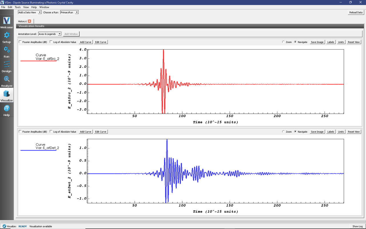
Fig. 288 The Visualize Window for the Dipole Source Illuminating a Photonic Crystal Cavity example
Further Experiments
By using the wideband source and examining the field strength detected below the crystal lattice, one may study the frequency response of this photonic crystal as one changes the device geometry, the dielectric constants, and the location and polarizations of the radiation source and detector.