Dielectric Waveguide with Gaussian Launcher (dielectricWaveguideGaussian.sdf)
Keywords:
- Photonic Waveguide, Unidirectional Mode Launcher, MAL,
- Guided Mode, Semiconductor
Problem description
The dielectric waveguide consists of a single, straight silicon waveguide that is parallel to the x-axis and centered at the origin. The waveguide is surrounded by silica. Matched Absorbing Layers (MALs) are used to dampen the E and B fields near the boundary of the simulation to suppress reflected fields.
A space gaussian source with the single frequency is used as a source and propagates in the +x direction.
This simulation can be performed with a VSimEM license.
Opening the Simulation
The dielectric waveguide example can be accessed from within VSimComposer through the following steps:
Select the New → From Example… menu item in the File menu.
In the resulting Examples window, expand the VSim for Electromagnetics option.
Expand the Photonics option.
Select Dielectric Waveguide with Gaussian Launcher and press the Choose button.
In the resulting dialog, create a New Folder if desired, and press the Save button to create a copy of this example.
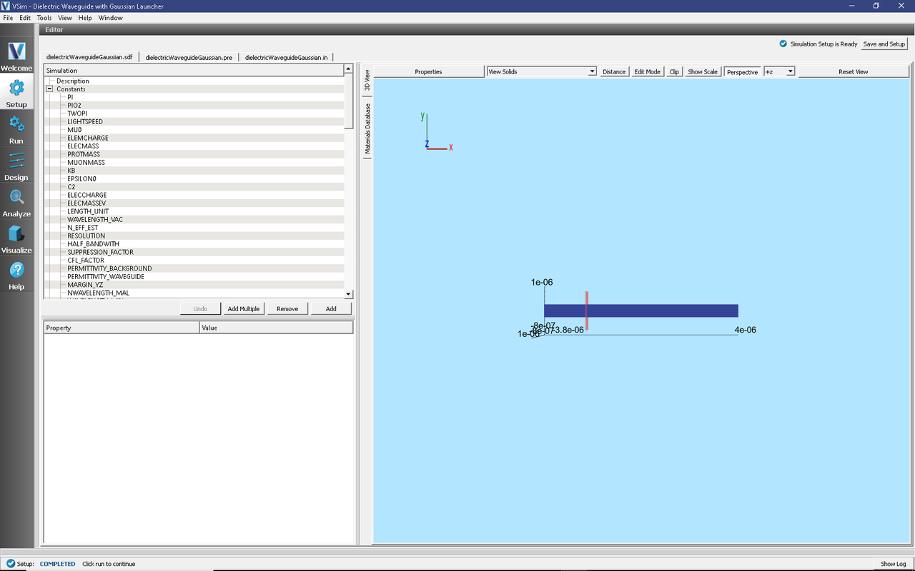
All of the properties and values that create the simulation will now be available in the Setup window as shown in Fig. 266. You can expand the tree elements and navigate through the various properties. The right pane shows a 3D view of the geometry, as well as the grid. To show or hide the grid, expand the Grid element and select or deselect the box next to Grid.

Fig. 266 The Setup window for the dielectric waveguide example showing some relevant constants.
Simulation Properties
This example contains a number of constants defined to make the simulation easily modifiable. Some relevant constants are listed below.
PERMITTVITY_WAVEGUIDE and PERMITTVITY_BACKGROUND: Relative permittivities of silicon and silica. These constants are used in multiple parameters and in the accompanying Python file for solving the waveguide modes.
WAVELENGTH_VAC: Wavelength of the input signal. This wavelength is also used for the calculation of the fundamental guided mode of the device.
NWAVELENGTH_MAL: Approximate number of wavelengths that can fit in a MAL region. The thickness of the MAL regions in this example are measured in wavelengths.
The Materials section contains just silicon and silica.
The Geometries includes the CSG waveguide and its defining parameters.
In Field Dynamics, there are FieldBoundaryConditions and CurrentDistributions to be aware of. In photonics simulations, Matched Absorbing Layers (MALs) are the most stable boundary conditions for preventing reflections. The gaussian approximation is defined under SpaceTimeFunctions and is set to drive the y-component of the currentSource.
Running the simulation
After performing the above actions, continue as follows:
Proceed to the Run Window by pressing the Run button in the left column. You will be asked to Save. Click Save.
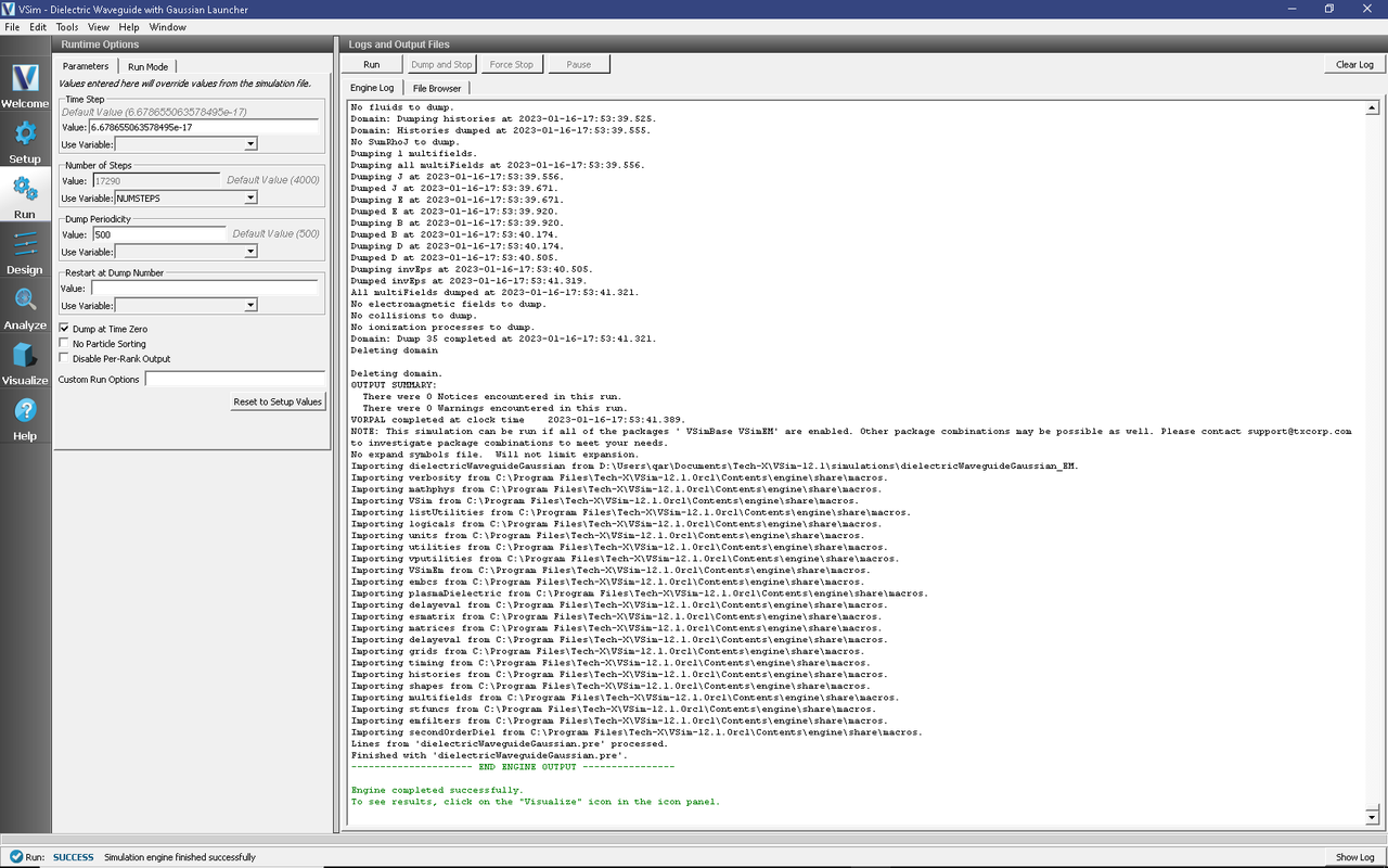
To run the file, click on the Run button in the upper left corner of the right pane. You will see the output of the run in the right pane. The run has completed when you see the output, “Engine completed successfully.” The result is shown in Fig. 267.

Fig. 267 The output after a successful run.
Visualizing the Results
Then proceed to the Visualize window by pressing the Visualize button in the left column.
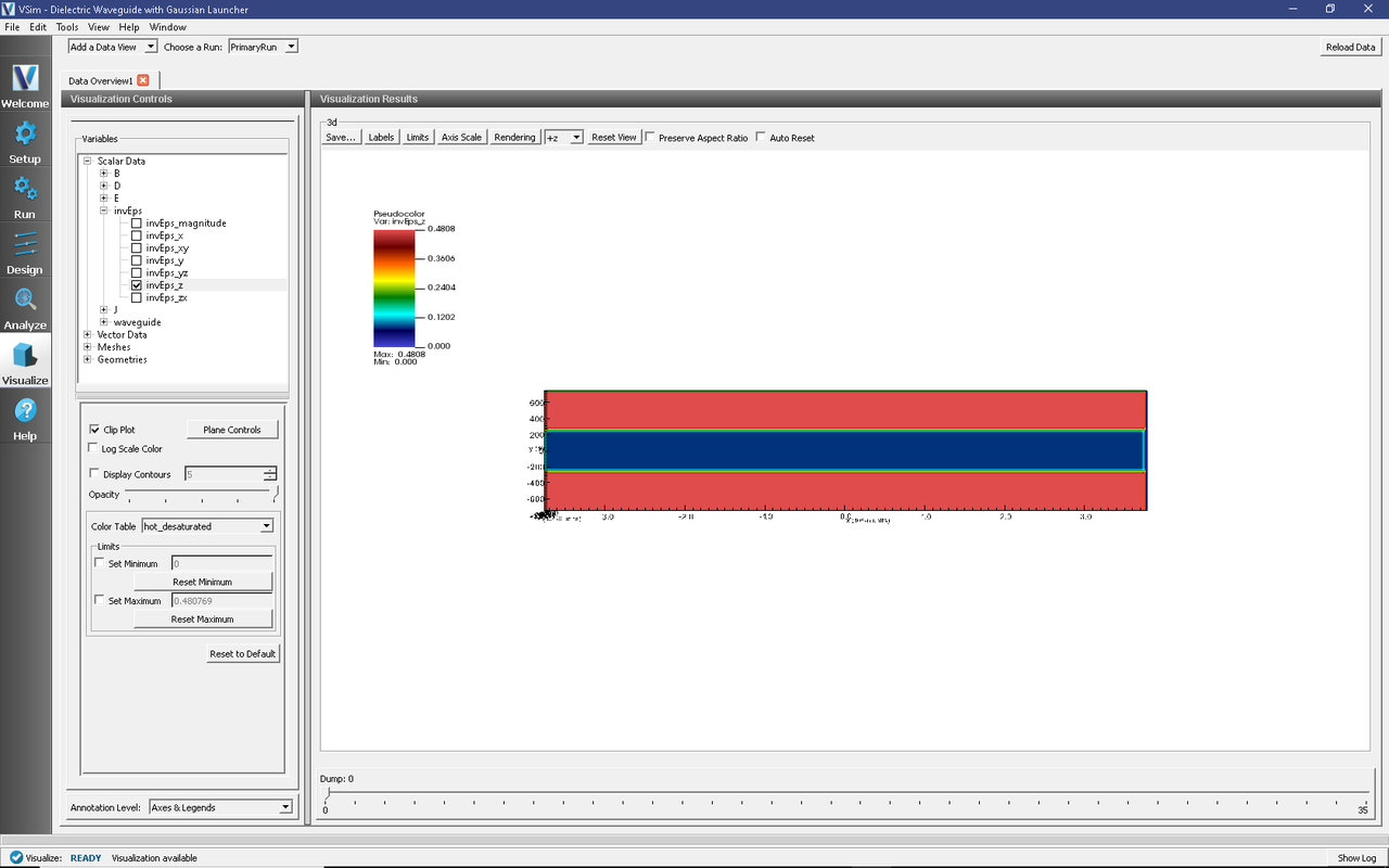
You can verify that the geometry is correct by visualizing the inverse permittivity as follows:
Near the top left corner of the window, make sure Data View is set to Data Overview.
Expand Scalar Data, expand invEps, and select invEps_z
In the controls below the variables frame, select Clip All Plots.
By default, the clipping plane is at z = 0, which is in the middle of dielectric waveguide structure height-wise. As such, this will reveal the dielectric waveguide’s 2D layout geometry as seen in Fig. 268.

Fig. 268 Visualization of inverse epsilon field’s Z component
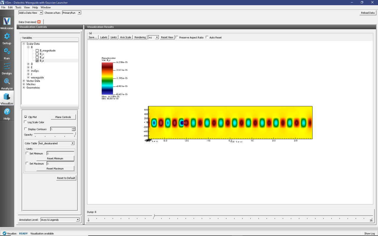
A useful visualization of the dielectric waveguide would be to view the Z component of the B field to qualitatively see the mode propagate down the waveguide.
Near the top left corner of the window, make sure Data View is set to Data Overview.
Expand Scalar Data, expand B, and select B_z
In the controls below the variables frame, select Clip All Plots.
Select the final dump step (dump 8) on the lower right of the screen using the slide bar. Fig. 269 shows an example of what one should expect if one has run the simulation for enough cycles.

Fig. 269 Visualization of the B field’s Z component
Further Experiments
One can experiment by changing constants or introducing a different signal to drive the waveguide.