Wafer Impact in Plasma Processing (waferImpact.sdf)
Keywords:
- uniform ion beam, wafer edge, RF voltage source, poisson solver, dielectric
Problem Description
This example illustrates how to use VSim to model a plasma processing problem in which argon ions are used to etch wafers used for microelectronics. In a typical chamber, the plasma is generated by imposing a voltage source at one of the boundaries which oscillates in the radio frequency (RF) range (a few MHz to tens of MHz). The plasma is generated as the electrons oscillate in response to the applied RF voltage and collisionally ionize the neutral Argon ions present in the chamber. In this example we are not interested in how the plasma forms and therefore pre-populate the simulation with electrons and Ar ions. During this process, a sheath forms near the wafer and the thickness of the sheath oscillates with the voltage RF source. The resulting Ar ions are then accelerated toward the wafer primarily by the sheath electric field and thereby etch the wafer. Unlike the electrons, which respond nearly immediately to the RF voltage source, the ions are accelerated more slowly and the motion of the ions can be found by averaging the sheath potential drop over one RF period. A desired outcome would be a uniform plasma sheath and therefore a uniform ion beam along the length of the wafer. One significant obstacle to this process occurs at the edge of the wafer, where changes in the dielectric material lead to modification to the sheath electric field.
The process described above is fundamentally a kinetic process involving processes on electron and ion time scales. However, simulation of the above process is mostly needed near the wafer edge where non-uniformities in the sheath potential cause problems. One solution to this problem is with the use of a so-called “focus ring” which is a second piece of dielectric material (e.g. quartz) of varying height placed next to the silicon wafer which is used to shape the sheath and make it more uniform at the edge of the wafer. Therefore, in this example we only simulate a region near the wafer edge and sufficiently far enough into the bulk of the plasma that the sheath dynamic is adequately resolved. As a result, we do not include most of the plasma far from the wafer and save significant computational time by modeling only the interesting and necessary processes.
Because we are not modeling most of the plasma, we have developed a method of injecting the plasma at the boundary opposite the wafer that is smooth and results in no artificial sheath at the computational boundary. An injection method is necessary to replace the plasma lost to the wafer and focus ring. The electrons and ions are injected using flux conserving particle boundary conditions accomplished through the use of a Space-Time Python Function (stPyFunc) which is a flexible way for the user to define their own function via a call external to Python. The particles are injected using a Slab Settable Flux boundary condition which correctly computes the initial position and velocity upon injection in the simulation domain.
The dielectric materials are modeled by constructing a CSG geometry in VSim. The user could easily import their own CAD (.stl or .step files) geometries and assign dielectrics to the various parts of the imported geometry. However, for this example, you can view the geometries by expanding “Geometries” and then expanding “CSG”. We then assign a dielectric material (and hence a dielectric constant) to each geometry, which is further explained below. A combination of Dirichlet and Neumann boundary conditions on the simulation boundaries are imposed. Field boundary conditions are imposed under Field Dynamics -> FieldBoundaryConditions. The plasma is represented by macro-particles which are evolved using the Boris scheme in a 2D cylindrical (z-r) coordinate system. The particle boundary conditions are Cut-Cell Accumulate which allows the electrons and ions to be absorbed by the dielectric material. The dielectric retains the accumulated charge once a plasma particle hits the dielectric. Averaged over one RF cycle, the total charge accumulation will be near-zero, but over short periods, the dielectric can have a net positive or negative charge.
We have also included critical diagnostics needed to determine the effect of the focus ring, collisions, and other physical processes crucial to this problem. One diagostic is the angular energy distribtuion (AED) function. We find that it is crucial to include collisions (even with a tenuous background gas) in order to obtain an AED function that is well centered around the normal to the wafer. We have also included a flux calculation to determine the uniformity of the ions impacting the wafer. The use of both of these diagnostics is discussed below.
This simulation can be run with a VSimPD license.
Opening the Simulation
The wafer impact example is accessed from within VSimComposer by the following actions:
Select the New → From Example… menu item in the File menu.
In the resulting Examples window expand the VSim for Plasma Discharges option.
Expand the Surface Interactions option.
Select Wafer Impact and press the Choose button.
In the resulting dialog, create a New Folder if desired, then press the Save button to create a copy of this example.
All of the properties and values that create the simulation are now available in the Setup Window as shown
in Fig. 650. Note that you can change the scale that is shown on the axes in the SetUp
window. In this case, the axes in Fig. 650 are shown in cm. You can change the scale
by clicking on the “Show Scale” button at the top of the SetUp window. You can expand the tree elements and navigate through the various properties,
making any changes you desire. Please note that many options are available by double clicking on an option and
also right clicking on an option. The right pane shows a 3D view of the geometry as well as the grid.
To show or hide the grid, expand the “Grid” element and select or deselect the box next to Grid. You can also
show or hide the different geometries by expanding the “Geometries” element and selecting or deselecting “Silicon_WaferUnionCurved_Silicon_End”
and/or “quartz_FR”. “Silicon_WaferUnionCurved_Silicon_End” is a union of “Curved_Silicon_End” and “Silicon_Wafer”.
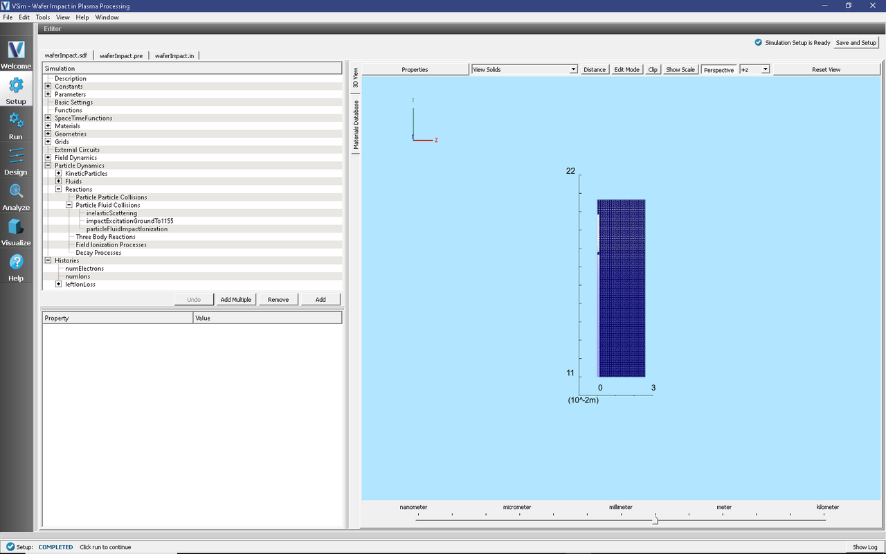
Fig. 650 Setup window for the wafer impact example.
Simulation Properties
This example contains many user defined Constants and Parameters which help simplify the setup and make it easier to modify. The following constants or parameters can be modified by left clicking on Setup on the left-most pane in VSim. Then left click on + sign next to Constants or Parameters and all the constants or parameters used in the simulation will be displayed. To add your own constant or parameter, right click on Constants or Parameters and left click on Add User Defined. Below is an explanation of a few of the constants and parameters used. There are several more constants and parameters included in the simulation.
QUARTZ_UPPERX/QUARTZ_LOWERX/QUARTZ_UPPERY/QUARTZ_LOWERY: Location of quartz focus ring in simulation domain
SILICON_UPPERX/SILICON_LOWERX/SILICON_UPPERY/SILICON_LOWERY: Location of silicon wafer in simulation domain
V0: Amplitude of RF voltage source
OMEGA_RF: Angular frequency of RF source. Linear frequency is OMEGA_RF/\(2\pi\)
NEUTRAL_PRESSURE_TORR: Pressure of neutral background gas. This determines the mean free path.
There are also many SpaceTimeFunctions (STFunc) defined in this example. vxRighte and vxRighti are space-time Python functions (stPyFunc) called from a Python script called “waferImpact.py”. In order for a Python function to be called correctly, the Python script must be given the same prefix as the input file, in this case “waferImpact”. The functions that are called are “EmitVxRighte” and “EmitVxRighti”. These functions invert the cumulative distribution function [BL04] given by \(v_x \times f(v_x)\), where \(f(v_x)\) is the initial distribution function which in this example is a drifting Maxwellian with the drift set to the ion acoustic speed. We use Rejection-Sampling theory to invert \(v_x \times f(v_x)\) since there is no analytic solution for a drifting Maxwellian.
In addition to the SpaceTimeFunctions, there are also several materials that need to be added. To open the materials data base, right click on “Materials”, then click on “import materials”. This will open a folder that you can use to open the material data base file. The default materials data base file is called “emthermal.vmat”. You don’t need to add any materials to the simulation for this example to run. The two dielectrics which are included in the simulation are quartz and silicon. However, you can also choose to add your own dielectric using the same format as the other materials already included.
To examine how the silicon wafer and quartz focus ring are modeled, expand “Geometries” by left-clicking on the + sign. Then expand “CSG”. There you see two geometries that have been assigned materials. The geometry called “Silicon_WaferUnionCurved_Silicon_End” is a bolean union between “Curved_Silicon_End” and “Silicon_Wafer”. This geometry has been assigned the material silicon. The geometry called “quartz_FR” is the focus ring and the dielectric material assigned to it is quartz. The dielectric constants for these two regions are automatically added to the Laplacian matrix used in the Poisson field solve. Note that in order to add dielectrics to your simulation when using the electrostatic field solve requires a VSimPD license.
We find that including collisions is crucial to this problem. Collisions tend to create an ion distribution that is centered around the normal to the wafer. Collision can be added to any VSim simulation by first navigating to “Basic Setting” in Composer. Before adding collisions, you must first double click next to “particles” and choose “include particles”. Once particles are added, double click next to “collisions framework” and choose “reactions”. Then in the elements tree, you will see a tab called “Particle Dynamics”. If you click the “+” icon to expand this options, you will see three options: “KineticParticles”, “Fluids”, and “Reactions”. The plasma particles are added under “KineticParticles”. The background Argon gas is modeled as a fluid. Finally, all the reactions we include (ionization, elastic scattering, and excitation) are placed under “Particle Fluid Collisions”.
Typically you want to run this simulation long enough for the ions to come to equilibrium, which can take between 10-100 RF cycles. The time step is automatically computed using a parameter called “DT” and the number of time steps in a RF period is computed in a parameter called “NT”. Therefore, multiplying NT by 10-100 will allow you to run the simulation for 10-100 RF cycles. In this example, we set the number of time steps to 10037 which is about 15 RF periods.
Running the Simulation
Once finished with the setup, continue as follows:
Proceed to the Run Window by pressing the Run button in the navigation column on the left.
To run the file, click on the Run button in the upper left corner of the Logs and Output Files pane.
You will see the output of the run in that pane. The run has completed successfully when you see the output, “Engine completed successfully.” This is shown in Fig. 651.
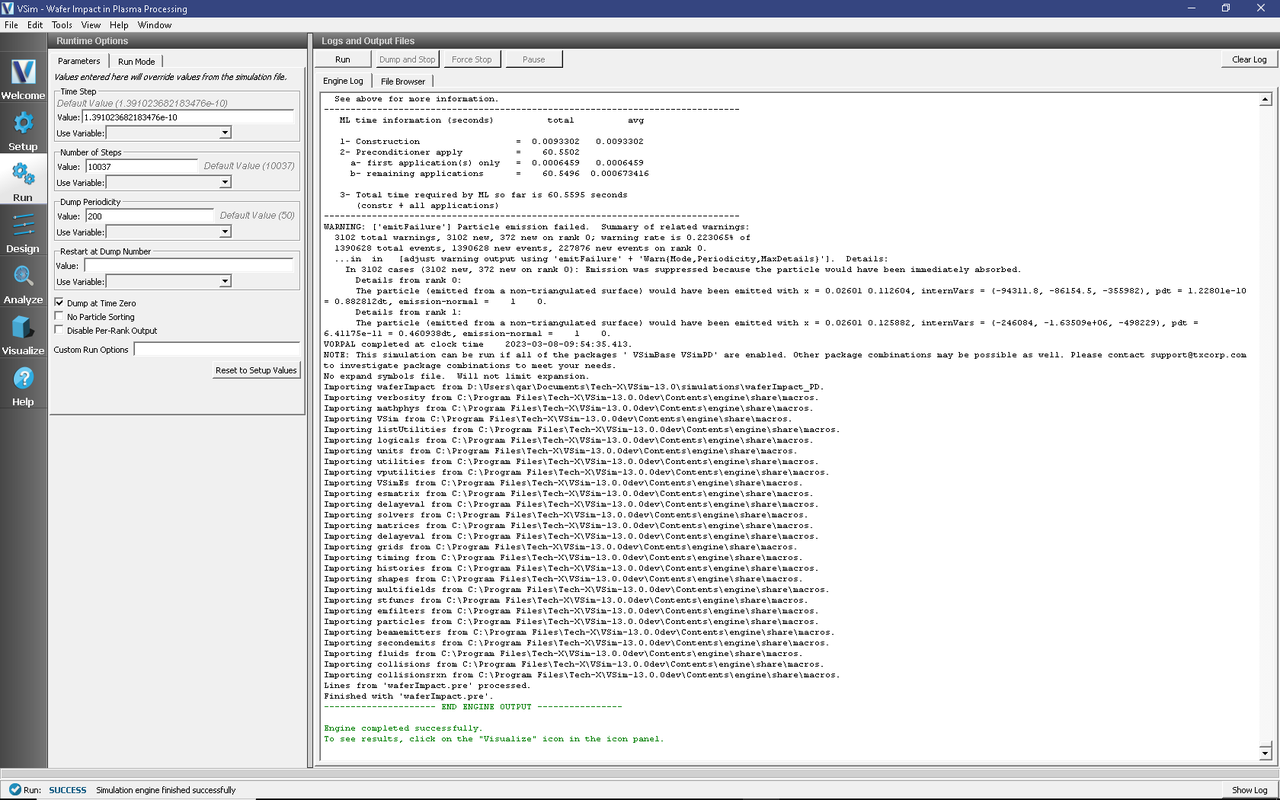
Fig. 651 The Run Window at the end of execution.
Analyzing the Results
A quantity of interest for many in plasma processing is the Angular Energy Distribution (AED) function. We have written an analyzer which computes the AED on any surface which saves the particle data in a history. The analyzer uses an “Absorbed Particle Log” history which in this simulation we call “leftIonLoss”. This history collects particle data on the silicon wafer at every time step. The Analyzer then specifies the region and time interval in which to bin the data in energy and angle, all of which the user specifies.
After the simulation has completed, continue as follows:
Proceed to the Analysis Window by pressing the Analyze button in the navigation column.
In the resulting list of Available Analyzers, select computeAED.py and press Open
The analyzer fields should be filled as below:
simulationName: “waferImpact”
speciesName: ions
startTime: 1.1170107212763709e-06
endTime: 1.3031791748224327e-06
lowerPos1: 0.155
upperPos1: 0.176
lowerPos2: 0 (ignored in 2D)
upperPos2: 1 (ignored in 2D
historyName: leftIonLoss
numEnergyBins: 25
numAngleBins: 26
lowerEnergy: 160
upperEnergy: 240
lowerAngle: -10
upperAngle: 10
NDIM: 2
perpDir: 0
normTan: if checked then history data are collected in norm-tangent coordinate system. If unchecked, simulation coordinate system is used.
“endTime” and “startTime” are times over which the AED is calculated in seconds. “perpDir” is the direction normal to the surface you are collecting the data on. A description of each input quantity is found in the VSim “Analyze” window.
Click Analyze in the top right corner.
The analysis is completed when you see the output shown in Fig. 652.
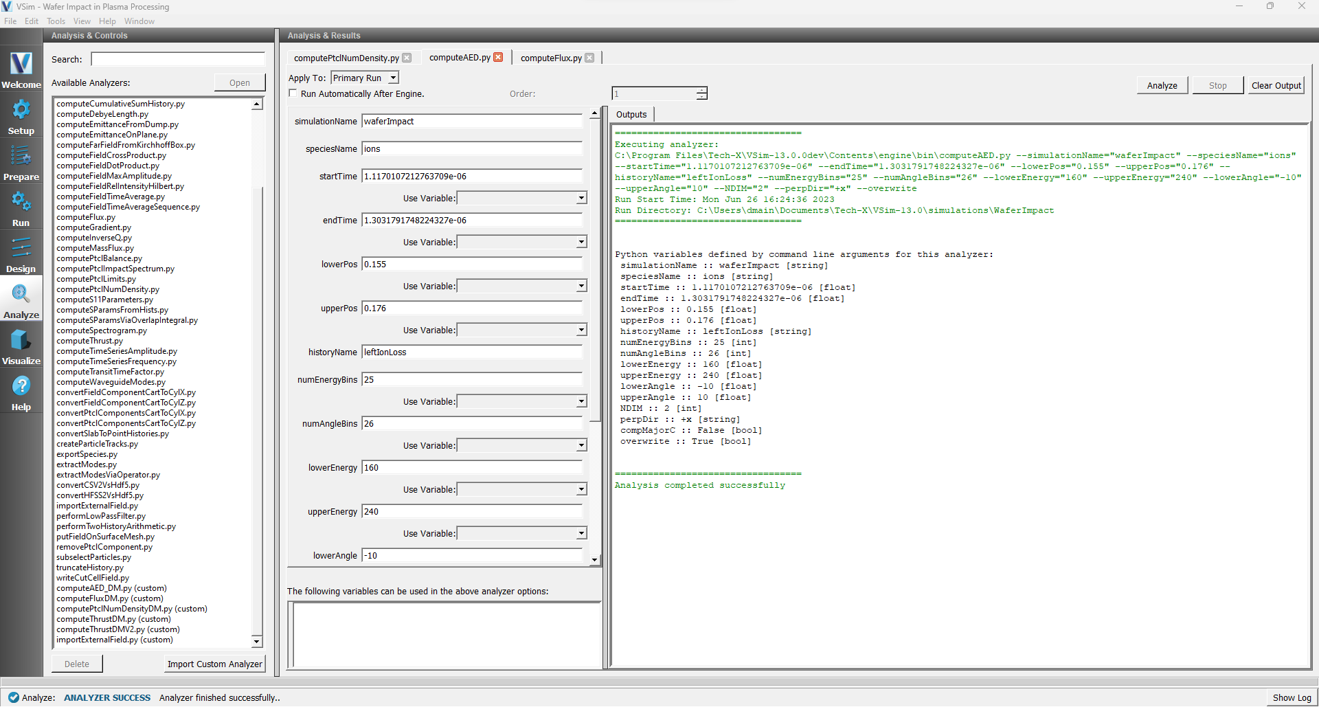
Fig. 652 The Analyze Window at the end of a successful run.
The resulting data is called ionsAED which is the probability distribution function normalized to 1 as a function of angle (in degrees) on the horizontal axis and energy (in eV) on the vertical axis.
Another quantity of interest in plasma processing is the spatial distribution of the number, energy, and charge flux impacting a surface. We have written an analyzer which computes the flux on any surface which saves the particle data in an “Absorbed Particle Log” history. In this simulation, the history is called “leftIonLoss”. This history collects particle data on the silicon wafer at every time step. The Analyzer then bins the data in position along the wafer. The user inputs the time interval and spatial region of interest.
After the simulation has completed, continue as follows:
Proceed to the Analysis Window by pressing the Analyze button in the navigation column.
In the resulting list of Available Analyzers, select computeFlux.py and press Open
The analyzer fields should be filled as below:
simulationName: “waferImpact”
speciesName: ions
startTime: 1.1170107212763709e-06
endTime: 1.3031791748224327e-06
lowerPos1: 0.155
upperPos1: 0.176
lowerPos2: 0 (dummy argument not used in 2D simulation)
upperPos2: 1 (dummy argument not used in 2D simulation)
historyName: leftIonLoss
numBins1: 50
numBins2: 25 (dummy argument not used in 2D simulation)
NDIM: 2
perpDir: 0
“endTime” and “startTime” are times over which the flux is calculated in seconds. “perpDir” is the direction normal to the surface you are collecting the data on. A description of each input quantity is found in the VSim “Analyze” window.
Click Analyze in the top right corner.
The analysis is completed when you see the output shown in Fig. 653.
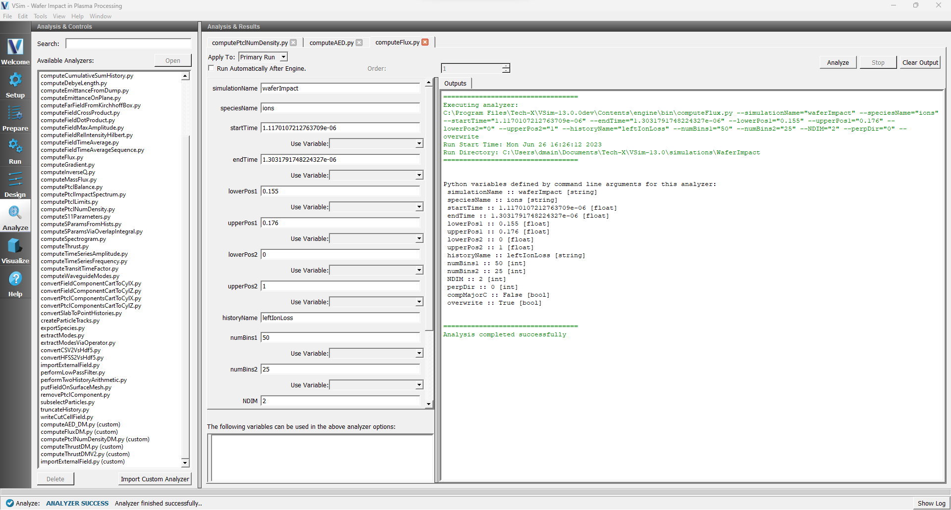
Fig. 653 The Analyze Window at the end of a successful run.
The resulting data are called ionsNumFlux, ionsEnergyFlux, and ionsCurrentFlux.
Visualizing the Results
After performing the above actions, the results can be visualized as follows:
Proceed to the Visualize Window by pressing the Visualize button in the navigation column.
Clicking on the Add a Data View dropdown menu shows there are many different types of data to visualize.
To get started, lets visualize the self-consistent potential.
Click on the Data Overview tab which is a default tab already loaded in the “Visualize” section of VSim.
Under Variables, expand “Scalar Data” then check the box called “Phi”
Finally, to visualize the potential in the context of the geometries in the simulation, expand “Geometries”, and check the boxes next to “poly(End)” and “poly(FR)”.
Slide the bar to the right at the bottom to view the potential and notice that the sheath thickness varies with time.
The resulting visualization is shown in Fig. 654.
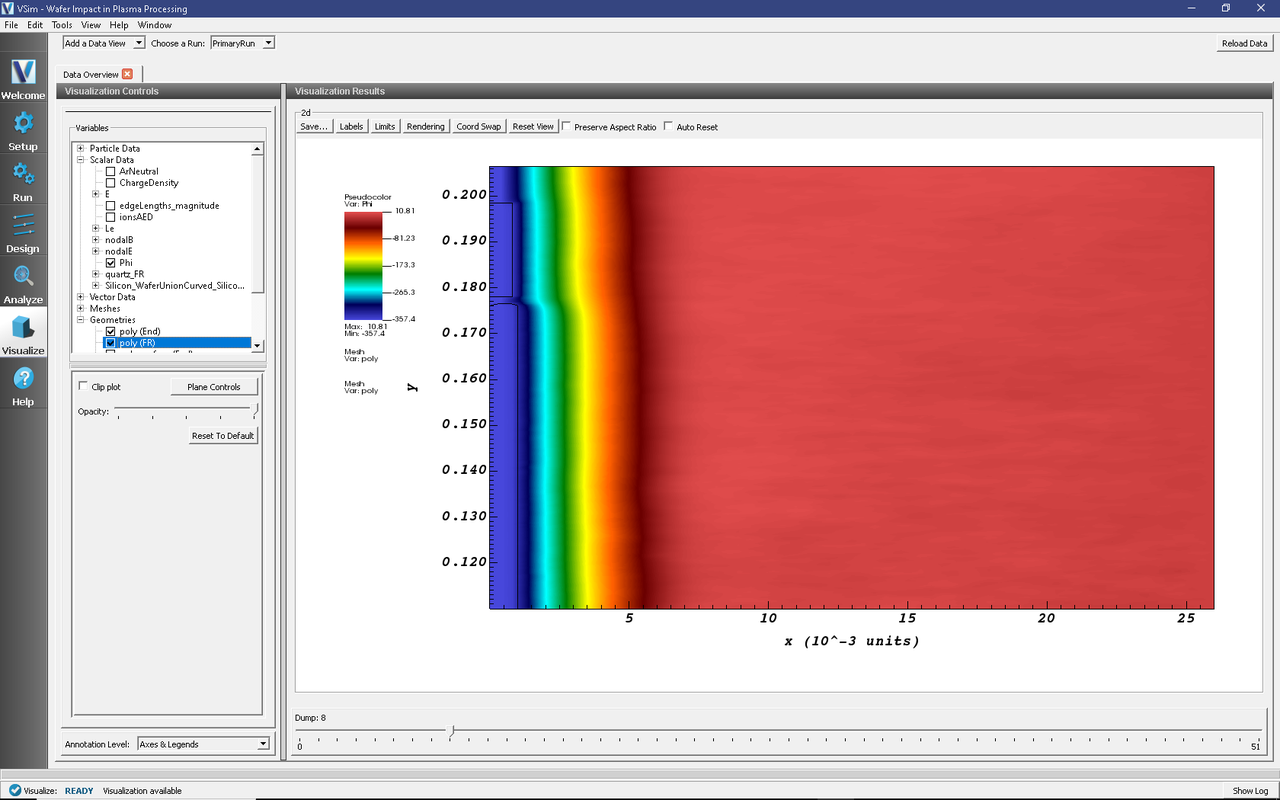
Fig. 654 The evolved potential with the geometries superimposed.
We now visual the Ion Angular Energy Distribution (IAED) function calculated in the previous section. Click on Add a Data View then click on Data Overview. In the newly created Data Overview tab, expand Scalar Data and check the box called “ionsAED”. The horizontal axis represents angle ranging from -10 degrees to 10 degrees. The vertical axis represents energy in eV ranging from 160 to 240 eV. You can make the color scale more sensitive by changing “Set Maximum” value to 0.01 on the left side of VSim Composer. The data are shown in Fig. 655.
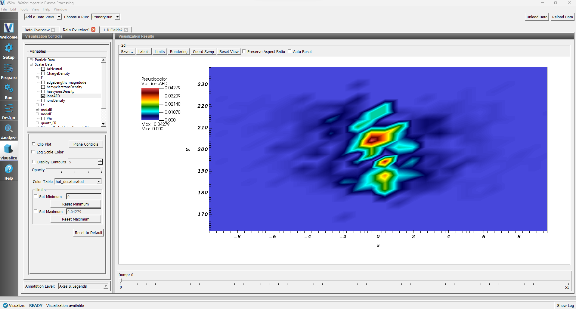
Fig. 655 Ion Angular Energy Distribution (IAED) function which was generated in the previous section.
When the AED is computed, the 1D Angular Distribution (AD) is computed by integrating over all energies. Likewise the 1D Energy Distribution (ED) is computed by integrating over all angles. These can be plotted by clicking on Add a Data View then clicking on 1-D Fields which will open a new tab. In “Graph 1” select ionsAD and in “Graph 2” select ionsED. The visualization window with the plots is shown in Fig. 656.
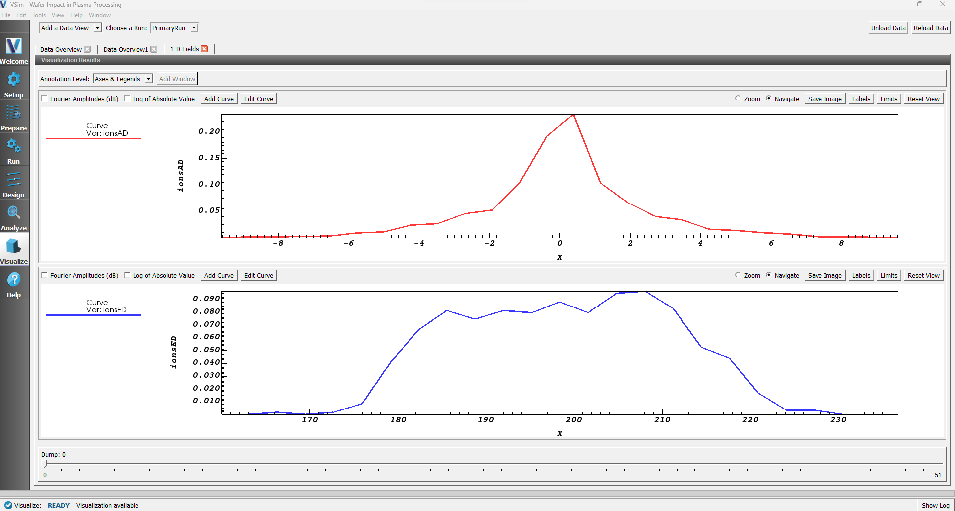
Fig. 656 Ion Angular Distribution (AD) and Energy Distribution (ED) functions which were generated in the previous section.
Finally we visualize the flux onto the wafer computed with “computeFlux.py” in the previous section. To view this data set, click on Add a Data View then click on 1-D fields. In the newly created 1-D Fields tab, click on “Add Curve” and choose “ionsNumFlux”. You will also see two other options corresponding to the energy flux and charge flux (i.e. current) onto the surface. The horizontal axis represents distance along the wafer. The vertical axis represents number flux. The data are shown in Fig. 657.
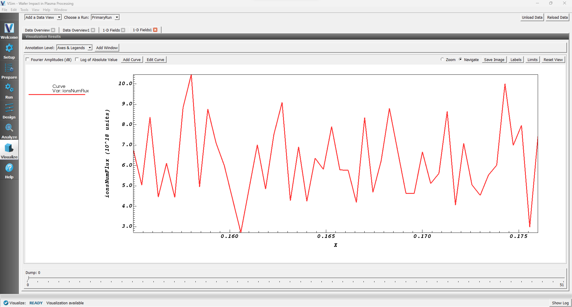
Fig. 657 Ion Number flux impacting the wafer. These data were computed with the analyzer computeFlux.py.
Further Experiments
For this simulation, collisions with a background neutral species have been included. You could include more excitation collisions to make the interaction with the background gas more realistic. You can also add secondary electron emission off of the dielectrics. Lastly, you can modify the RF source or add an additional RF source to create a dual frequency RF source.